Micromechanical device having two sensor patterns

a micromechanical and sensor pattern technology, applied in the direction of measuring devices, fluid pressure measurement by mechanical elements, instruments, etc., can solve the problems of multi-sensor requirements, inability to represent on one chip in a monolithically integrated manner, and relatively high cost of multi-chip applications, so as to reduce the cost and the required space, improve the functionality, and reduce the effect of connection paths

Active Publication Date: 2009-07-07
ROBERT BOSCH GMBH
View PDF16 Cites 21 Cited by
  • Summary
  • Abstract
  • Description
  • Claims
  • Application Information

AI Technical Summary

Benefits of technology

[0002]The micromechanical device according to the present invention has the advantage of providing a first and a second sensor pattern on a shared semiconductor material in a monolithically integrated manner, which not only reduces the cost and the required space but also improves the functionality due to smaller connection paths, lower transition resistances, etc., and allows a more cost-effective overall solution through the use of the same converter principle, i.e., a piezoresistive converter principle, in particular, for both sensor patterns. It is also possible to monolithically integrate both sensor patterns with a single, two-channel evaluation circuit, so that the production expense for the micromechanical device is lower on the one hand, and the evaluation of the generated signals is improved on the other hand.
[0003]It is particularly advantageous that the converter principle is based on the piezo-sensitive effect, in particular the piezoresistive effect, in a plurality of sensor regions of the semiconductor material. In an especially advantageous manner this makes it possible to combine high sensitivity of the sensor patterns with a cost-effective production method of the micromechanical device. Furthermore, a converter principle on the basis of the piezoresistive effect is less susceptible to the problems caused by static charges, so that the device according to the present invention is able to be configured in a more fail-safe manner. In addition, it is preferred that the first sensor pattern has a first diaphragm introduced into the semiconductor material, and that the second sensor pattern has a second diaphragm introduced into the semiconductor material, each diaphragm preferably including at least one sensor region or being connected to at least one sensor region.
[0004]By the use of the diaphragms the present invention provides a simple and robust possibility for producing a pattern that is sensitive to a mechanical influence variable, so that sensor patterns that are especially robust and reliable are able to be produced on the basis of the piezoresistive converter principle. Furthermore, it is preferred if the first sensor pattern has a hermetically sealed first cavity underneath the first diaphragm and / or the second sensor pattern has a seismic mass connected to the second diaphragm, the seismic mass preferably being hermetically encapsulated and / or the second diaphragm being provided with support, in particular being supported by at least one lateral constriction. With relatively little effort and by using patterns that are producible in a robust manner, it is thus possible to realize a pressure sensor and a sensor which are sensitive to an inertial force, in particular an acceleration sensor for measuring a linear acceleration or for measuring an angular acceleration or a rate of rotation. Supporting the diaphragm prevents the sensor diaphragm from adhering to the underlying substrate when the cavity is produced inside which a vacuum exists at least in the meantime.
[0005]According to the present invention, it is especially advantageous that a circuit pattern of an electronic circuit for analyzing and / or processing signals emanating from the sensor patterns or being modified by the sensor patterns is introduced into the semiconductor material, the production of the circuit pattern preferably being at least partially provided simultaneously with the production of the sensor patterns. This makes it possible to produce a complete, combined sensor or a complete, combined sensor unit, which not only has the patterns that are sensitive to the mechanical variables to be measured, but which also implements preprocessing of the sensor signals, possibly even with a certain intelligence. Intelligent preprocessing in this context is understood to mean that a relation is already established between the signals emanating from the sensor patterns measuring the different mechanical variables, so that, for instance, implausible combinations of pressure and acceleration values are either not forwarded or their implausibility is at least indicated or signaled. According to the present invention, it is especially preferred that the diaphragms essentially include a monocrystalline material, preferably monocrystalline silicon. This allows an especially cost-effective production of piezo sensors that already respond to slight deflections of the diaphragm and thus operate with an especially high sensitivity.
[0006]In contrast to the related art, the method according to the present invention has the advantage that the diaphragms for the first sensor pattern and also for the second sensor pattern for the measurement of two different mechanical variables, especially pressure and linear acceleration, are produced simultaneously, so that the production of the device according to the present invention is able to be realized in an especially cost-effective manner. It is particularly advantageous that the seismic mass is made of substrate material, i.e., the semiconductor material. Furthermore, in the method according to the present invention it is preferred that a partial region of the semiconductor material is etched so as to become porous for the introduction of the diaphragms into the semiconductor material, preferably at a porosity of more than 50%, preferably more than 80%, and the first cavity and a second cavity are formed by relocating or etching out the semiconductor material in the partial region etched so as to become porous. According to the present invention, this advantageously makes it possible to produce the cavities without the introduction of accesses and without the use of undercut-type etching methods. Furthermore, according to the present invention it is advantageous that an etch barrier layer, preferably silicon oxide, is introduced into the second cavity in the region of the seismic mass to be formed, once the second cavity has been formed. The patterning of the seismic mass may thus be implemented in an especially precise manner from the rear of the semiconductor material, preferably utilizing a bulk-micromechanical processing sequence.
[0007]Another subject matter of the present invention is a combined acceleration and pressure sensor having a micromechanical device according to the present invention, the combined acceleration and pressure sensor having the advantage that, due to the use of the same—preferably a piezoresistive—converter principle for both sensings, a cost-effective overall solution through a single, two-channel evaluation ASIC is possible and, overall, either only two chips are required for the combined acceleration and pressure sensor, or a monolithic integration of the two sensor patterns together with the evaluation circuit is even possible. Furthermore, using the acceleration and pressure sensor according to the present invention, the detection of different components of the linear acceleration or the angular acceleration is possible, for instance the detection of a linear acceleration perpendicular to the substrate plane of the device, or an angular acceleration parallel to the substrate plane of the device. The substrate plane corresponds to the plane of the largest extension of the semiconductor material.

Problems solved by technology

It is disadvantageous that a plurality of sensors is required to measure several different mechanical variables, for instance to measure a pressure and an acceleration, the sensors furthermore generally being based on different converter principles and therefore unable to be represented on one chip in a monolithically integrated manner.
However, such multi-chip applications are relatively cost-intensive, which is to be avoided according to the present invention.

Method used


Image

  • Micromechanical device having two sensor patterns
  • Micromechanical device having two sensor patterns
  • Micromechanical device having two sensor patterns

Examples


Embodiment Construction

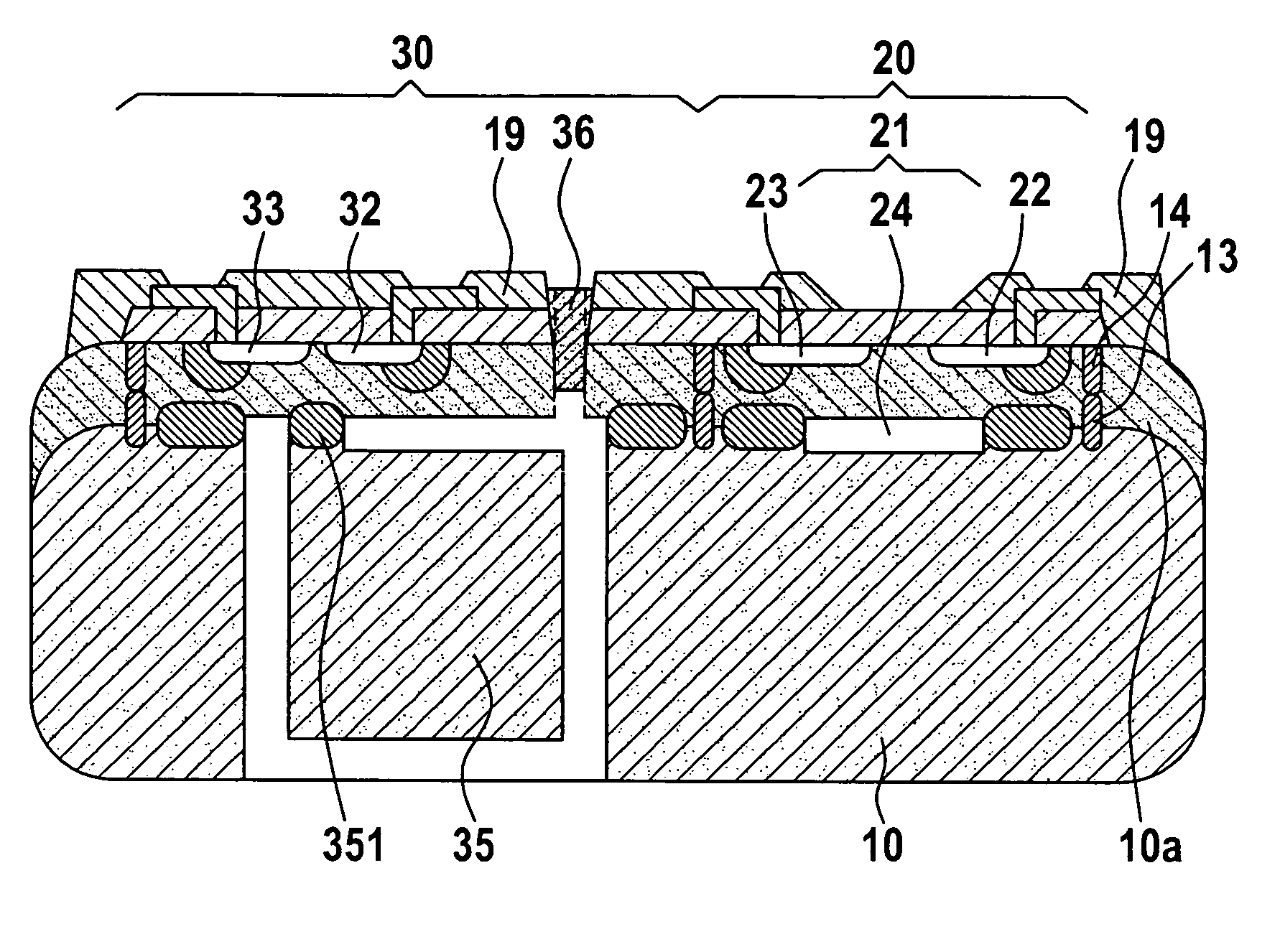
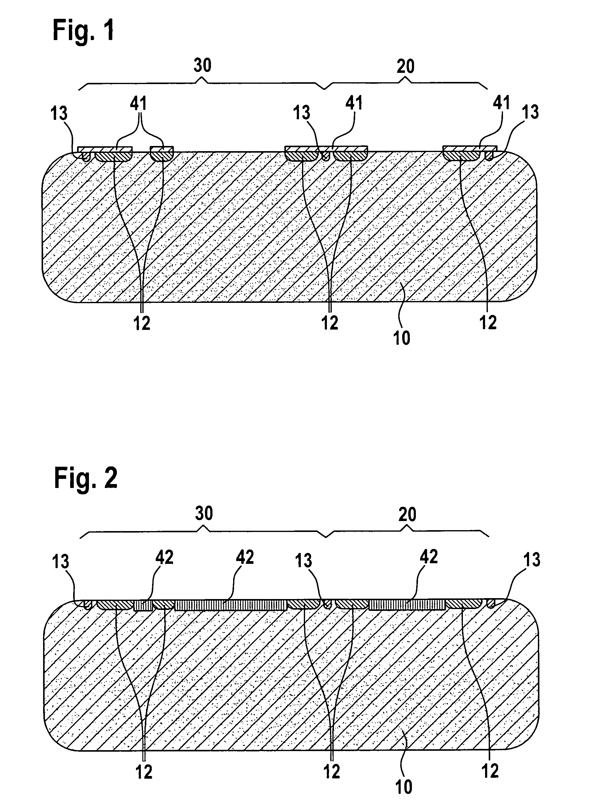
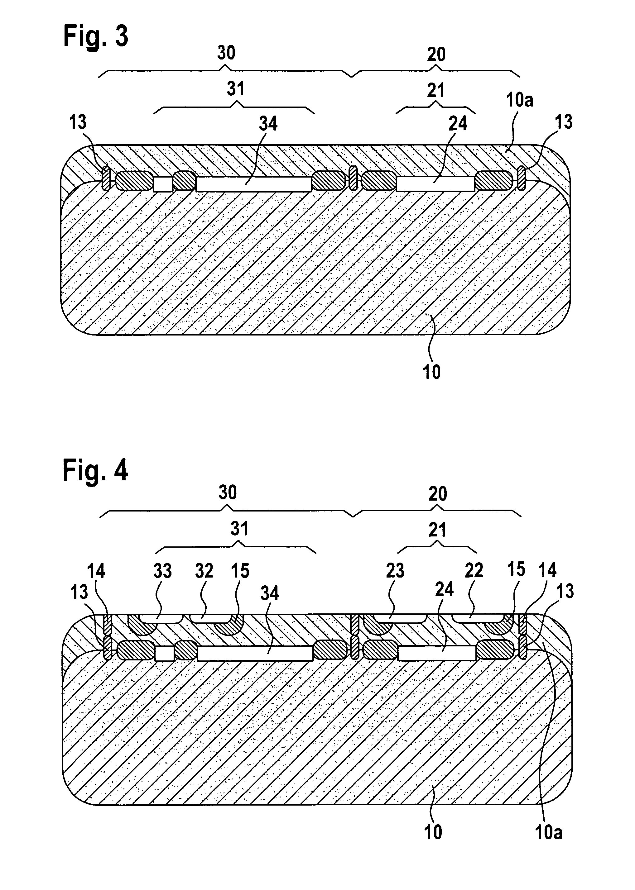
[0012]FIG. 1 shows a first preliminary pattern for a micromechanical device according to the present invention. Various doping regions 12 are introduced into a semiconductor material 10, which is provided as silicon wafer, in particular. According to the present invention, semiconductor material 10 is a p-substrate, for instance, and the introduced dopings 12 are relatively heavily negatively doped doping regions. Additional doping regions are likewise introduced into semiconductor material 10 as so called first well doping regions 13 and provide electrical insulation between different regions or patterns of semiconductor material 10. For instance, a first region 20 and a second region 30 are already discernable in FIG. 1 in which a first sensor pattern 20 and a second sensor pattern 30, respectively, will be realized in the finished micromechanical device according to the present invention, as will result from the description of the following figures. In a subsequent step, masks 41...


PUM

PropertyMeasurementUnit
porosityaaaaaaaaaa
porosityaaaaaaaaaa
pressureaaaaaaaaaa

Abstract

A micromechanical device and a method for producing this device are provided, two sensor patterns being provided in the semiconductor material to record two mechanical variables, in particular the pressure and the acceleration. The functionality of both sensor patterns is based on the same predefined converter principle.

Description

BACKGROUND INFORMATION[0001]German Patent Application No. DE 103 23 559 describes a micromechanical device, in particular a pressure sensor, the functionality of the sensor pattern of the pressure sensor being based on a piezoresistive converter principle for converting a mechanical force into an electrical signal. It is disadvantageous that a plurality of sensors is required to measure several different mechanical variables, for instance to measure a pressure and an acceleration, the sensors furthermore generally being based on different converter principles and therefore unable to be represented on one chip in a monolithically integrated manner. Applications in which simultaneous recording of a plurality of different mechanical variables, in particular pressure and acceleration, is desirable, are found in the measurement of tire pressures or also in side impact sensing in the automotive field. When sensors that are based on different converter principles are used to measure these ...

Claims


Application Information

Patent Timeline
Patent Type & Authority Patents(United States)
IPC IPC(8): G01L7/00G01P15/00
CPCG01L19/0092G01L9/0054
Inventor BENZEL, HUBERTSCHELLING, CHRISTOPH
Owner ROBERT BOSCH GMBH
Why Eureka
Try Eureka