Dicing method using an encased dicing blade submerged in cooling water
a technology of cooling water and dicing blade, which is applied in the direction of fine working devices, manufacturing tools, electric devices, etc., can solve the problems of chipping and cracking of semiconductor devices, and achieve the effect of reducing the discharge rate of cooling water, reducing the chipping of semiconductor devices, and reliable supply of cooling water
- Summary
- Abstract
- Description
- Claims
- Application Information
AI Technical Summary
Benefits of technology
Problems solved by technology
Method used
Image
Examples
embodiment 1
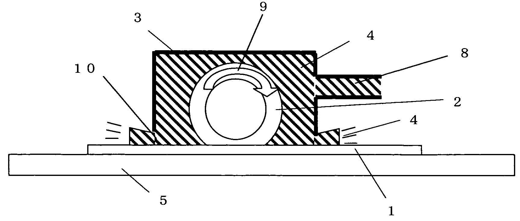
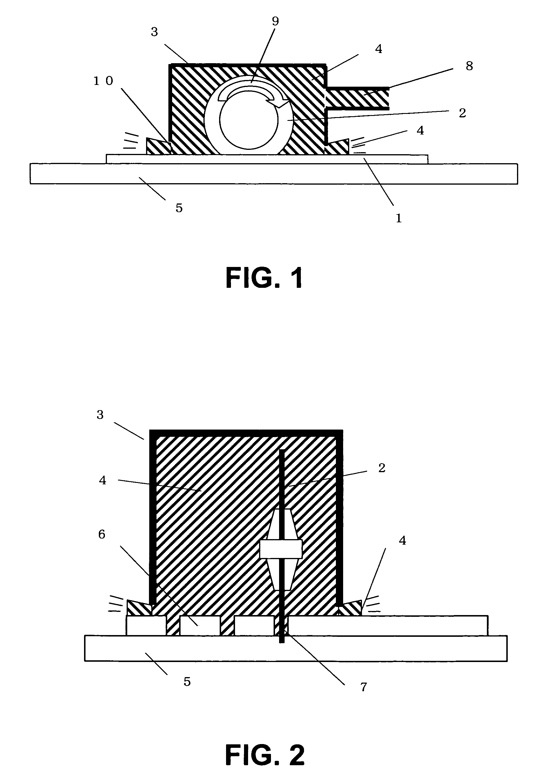
[0021]A dicing method according to a first embodiment of the present invention will be described with reference to FIGS. 1 and 2. FIG. 1 is a side view of a dicing device main portion including a dicing blade. FIG. 2 is an enlarged front view of the main portion. A semiconductor wafer 1 is bonded to a dicing tape 5 and is held on a wafer stage portion (not shown) of the dicing device. The semiconductor wafer 1 which is held is cut due to a rotation 9 of a dicing blade 2, to thereby provide individual semiconductor chips 6. As shown, the dicing blade is surrounded and encased by a case 3 filled with a liquid cooling medium in the form of cooling water 4 and is entirely submerged in the cooling water 4 except for the lower peripheral portion of the dicing blade 2 that protects outward from a bottom of the case 3. In FIGS. 1 and 2, the case 3 surrounds the dicing blade 2 with five flat surfaces of the case 3, including an upper surface, two front surfaces, and two side surfaces. As lon...
embodiment 2
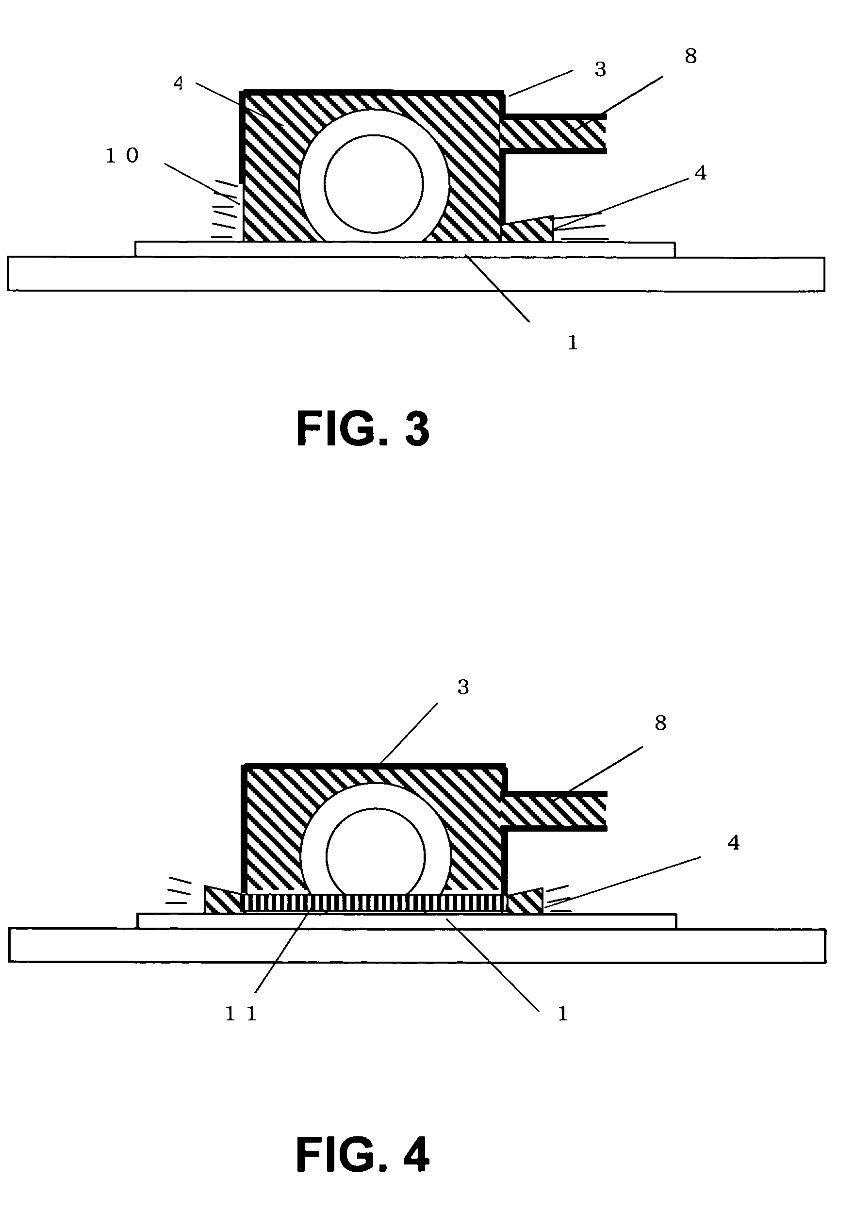
[0022]FIG. 3 shows a second embodiment of the present invention. The accumulation of cutting powder around the cutting point accelerates heat generation, leading to the decrease of cutting performance, which causes chipping and cracking in the semiconductor chip. Prompt dispersion of the cutting powder generated by cutting the wafer into the cooling water to be discharged out of the case is thus desirable. In order to achieve this, a size of the gap 10 between the surface of the semiconductor wafer 1 and the case 3 is adjusted, thereby making it possible to rapidly discharge the cooling water 4 including the cutting powder to the outside of the case. A large opening in the gap 10 increases the discharge rate of the cooling water and the cutting powder, enabling the cutting in the cooling water of a high degree of purity. On the other hand, a small opening in the gap 10 assures the proper water pressure in the case 3, thereby making it possible to promote the cooling of the dicing pl...
embodiment 3
[0023]FIG. 4 shows a third embodiment of the present invention. A brush 11 is provided in a gap between the surface of the semiconductor wafer 1 and the case 3, thereby reducing the discharge rate of the cooling water discharged from the gap and ensuring a water pressure in the case to allow the cooling water to be sufficiently supplied to the cutting point. Note that, it is preferable that a tip of the brush does not come into contact with the surface of the wafer and a slight space is maintained therebetween.
PUM
| Property | Measurement | Unit |
|---|---|---|
| speed | aaaaa | aaaaa |
| pressure | aaaaa | aaaaa |
| size | aaaaa | aaaaa |
Abstract
Description
Claims
Application Information
 - R&D
- Intellectual Property
- Life Sciences
- Materials
- Tech Scout
- Unparalleled Data Quality
- Higher Quality Content
- 60% Fewer Hallucinations
Browse by: Latest US Patents, China's latest patents, Technical Efficacy Thesaurus, Application Domain, Technology Topic, Popular Technical Reports.
© 2025 PatSnap. All rights reserved.Legal|Privacy policy|Modern Slavery Act Transparency Statement|Sitemap|About US| Contact US: help@patsnap.com


