Solid state imaging device
a solid-state imaging and imaging device technology, applied in the direction of semiconductor devices, radio-controlled devices, electrical devices, etc., can solve problems such as degradation of modulation transfer functions, and achieve the effect of suppressing signal charge diffusion
- Summary
- Abstract
- Description
- Claims
- Application Information
AI Technical Summary
Benefits of technology
Problems solved by technology
Method used
Image


Examples
first embodiment
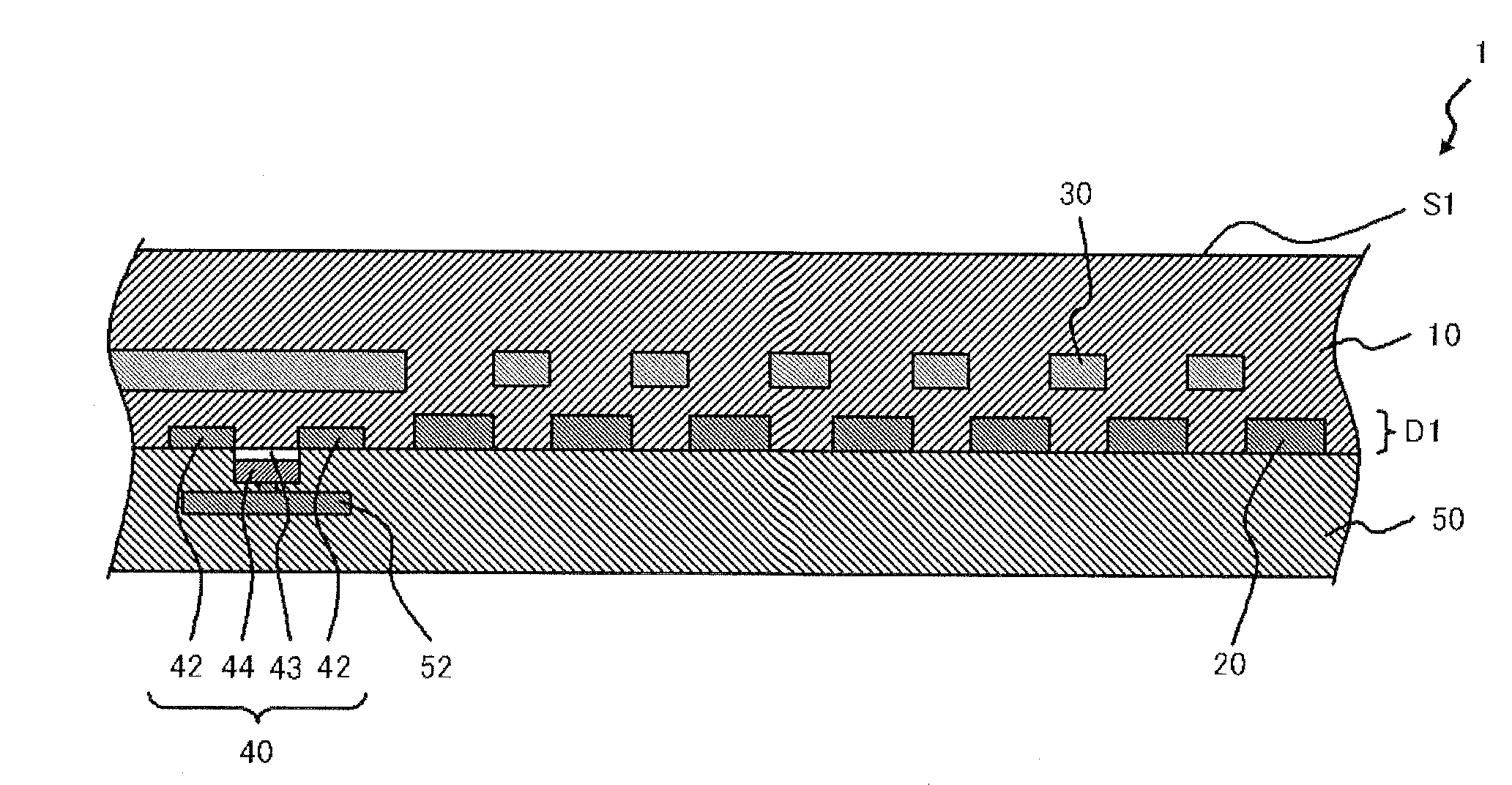
[0020]FIG. 1 is a cross-sectional view showing a solid-state imaging device according to a first embodiment of the present invention. The solid-state imaging device 1 includes a semiconductor substrate 10, photodetector elements 20, and blocking layers 30. In this embodiment, the semiconductor substrate 10 is a P type silicon substrate. The solid-state imaging device 1 receives light on the back surface thereof, and photoelectrically converts the light incident upon the back surface S1 of the semiconductor substrate 10, to thereby acquire an image of an object to be imaged.
[0021]The semiconductor substrate 10 includes a plurality of photodetector elements 20 aligned at a predetermined interval. More specifically, the photodetector elements 20 are located in the surface layer on the upper surface of the semiconductor substrate 10 (opposite to the back surface S1). The photodetector elements 20 serve to receive a signal charge generated through the photoelectric conversion. In this em...
second embodiment
[0032]FIG. 3 is a cross-sectional view showing a solid-state imaging device according to a second embodiment of the present invention. The solid-state imaging device 2 includes the semiconductor substrate 10, the photodetector elements 20, and the blocking layers 30. In the solid-state imaging device 2, the structure of the blocking layer 30 is different from that in the solid-state imaging device 1 shown in FIG. 1. The structure of the remaining portion of the solid-state imaging device 2 is substantially the same as that of the solid-state imaging device 1.
[0033]In this embodiment the blocking layer 30 extends into an inner part of the semiconductor substrate 10, from the back surface S1 thereof. In other words, an end portion of the blocking layer 30 is exposed on the back surface S1, and the other end portion is buried inside the semiconductor substrate 10.
[0034]A difference between the solid-state imaging device 1 and the solid-state imaging device 2 may be described as follows...
third embodiment
[0036]FIG. 4 is a cross-sectional view showing a solid-state imaging device according to a third embodiment of the present invention. The solid-state imaging device 3 includes the semiconductor substrate 10, the photodetector elements 20, and the blocking layers 30. In the solid-state imaging device 3, the structure of the blocking layer 30 is different from that in the solid-state imaging device 1 shown in FIG. 1. The structure of the remaining portion of the solid-state imaging device 3 is substantially the same as that of the solid-state imaging device 1.
[0037]In this embodiment the blocking layer 30 extends into an inner part of the semiconductor substrate 10, from the upper surface thereof. In other words, an end portion of the blocking layer 30 is exposed on the upper surface, and the other end portion is buried inside the semiconductor substrate 10.
[0038]A difference between the solid-state imaging device 1 and the solid-state imaging device 3 may be described as follows. In ...
PUM
 Abstract
Description
Claims
Application Information