
Low-frequency bias power in HDP-CVD processes

a technology of cvd process and low-frequency bias, which is applied in the direction of vacuum evaporation coating, plasma technique, coating, etc., can solve the problems of arcing within the chamber, poor gapfill ability, and difficult to completely fill high-aspect-ratio gaps using conventional cvd techniques, so as to reduce the risk of bias discharge and enhance the tuning speed of the bias system

Inactive Publication Date: 2009-08-11
APPLIED MATERIALS INC
View PDF10 Cites 4 Cited by
  • Summary
  • Abstract
  • Description
  • Claims
  • Application Information

AI Technical Summary

Benefits of technology

This approach reduces the occurrence of bias-induced discharges, enabling more efficient deposition of silicon oxide films with improved gapfill capabilities, even at lower chamber pressures and higher bias powers, thus enhancing the quality of semiconductor fabrication.

Problems solved by technology

One persistent challenge faced by semiconductor manufacturers in the design and fabrication of such densely packed integrated circuits is the desire to prevent spurious interactions between circuit elements, a goal that has required ongoing innovation as geometry scales continue to decrease.
High-aspect-ratio gaps are difficult to fill completely using conventional CVD techniques, which tend to have relatively poor gapfill abilities.
One drawback to biasing the substrate is that an electrical discharge may result, causing arcing within the chamber.
Even when such discharges are relatively small, they may result in microcontamination of the substrate and produce defects.
Although lower chamber pressures and higher bias powers may be useful in achieving desired film characteristics, such as substantially void-free gapfill for certain aggressive structures, they both tend to increase the occurrence of undesirable bias discharge.

Method used


Image

  • Low-frequency bias power in HDP-CVD processes
  • Low-frequency bias power in HDP-CVD processes
  • Low-frequency bias power in HDP-CVD processes

Examples


Embodiment Construction

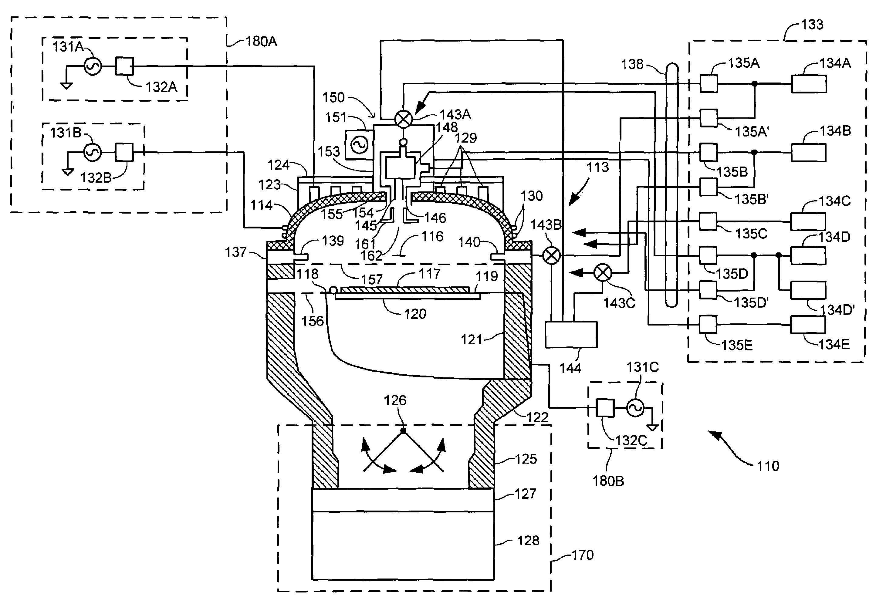
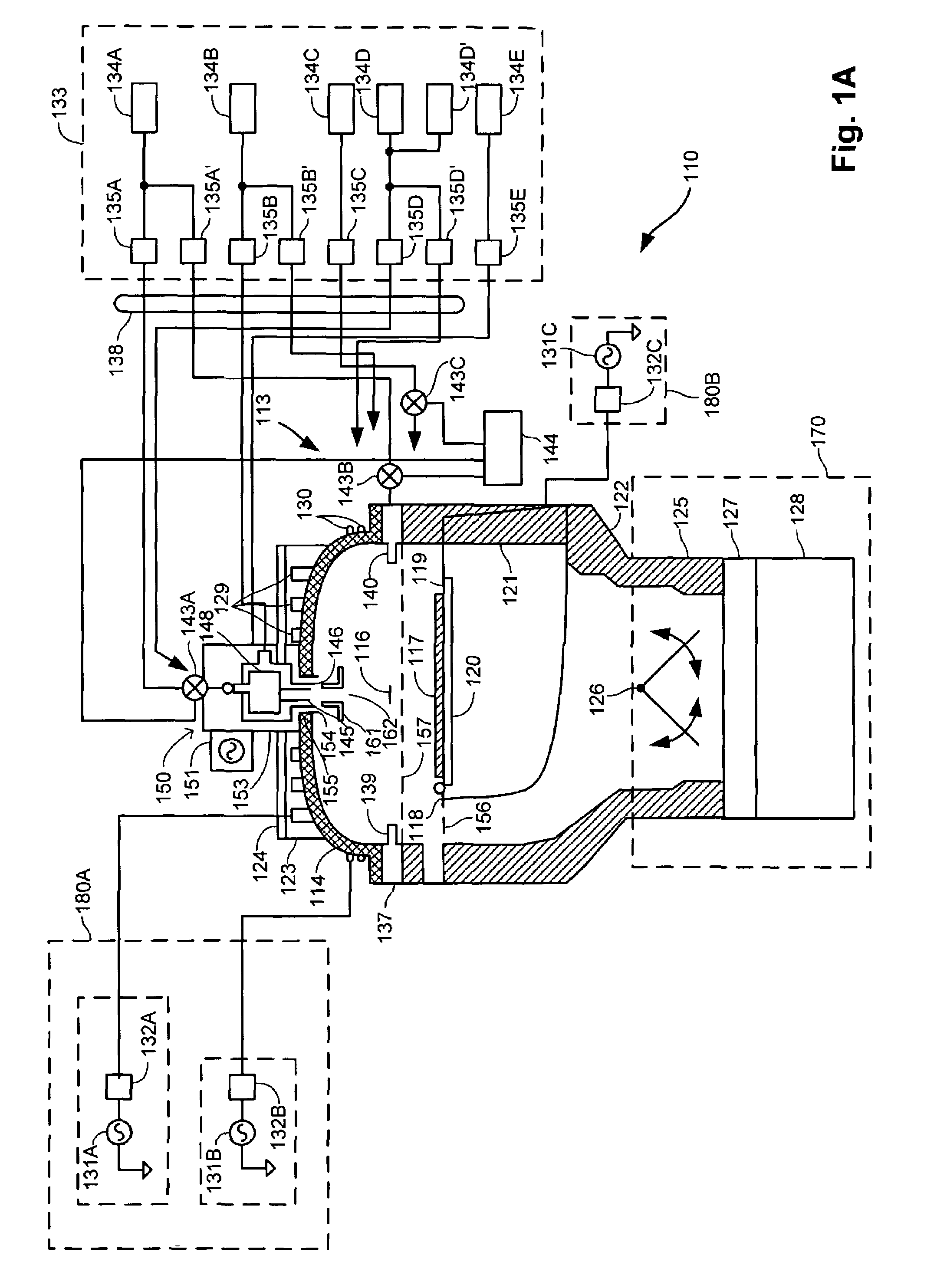
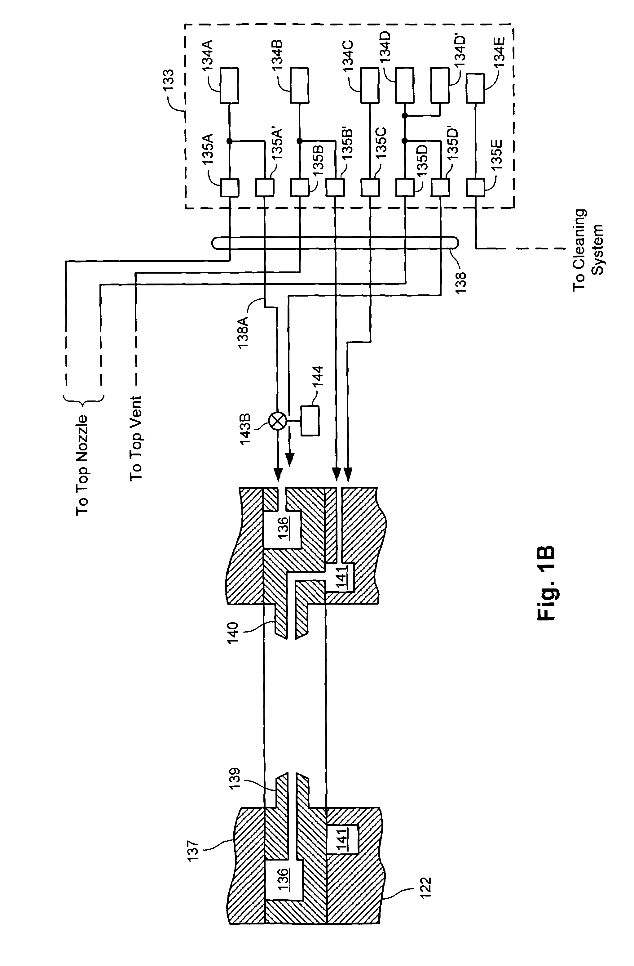
[0020]The inventors have recognized that the risk of bias discharge during HDP-CVD processes may be reduced by operating an rf bias generator at lower frequencies. Current HDP-CVD systems typically operate rf bias generators at a frequency of about 13.56 MHz, a value that has been chosen primarily to avoid frequency bands that are commonly used for commercial and military applications. Besides changing ion energy and angle distributions in the plasma, the reduction of bias frequency is also believed to influence coupling RF power with ions in plasma such that lower chamber pressures and higher biases may be used. In particular, the response capability of ionic species is limited so that individual ions do not respond to the bias field as effectively when the field changes rapidly. When higher frequencies are used, the power coupling with the ions is thus relatively inefficient, leading to heating of the plasma. The combination of the high density of the plasma with an elevated plasm...


PUM

PropertyMeasurementUnit
frequencyaaaaaaaaaa
frequencyaaaaaaaaaa
poweraaaaaaaaaa

Abstract

A substrate processing system has a housing that defines a process chamber. A substrate holder disposed within the process chamber supports a substrate during substrate processing. A gas-delivery system introduces a gas into the process chamber. A pressure-control system maintains a selected pressure within the process chamber. A high-density plasma generating system forms a plasma having a density greater than 1011 ions / cm3 within the process chamber. A radio-frequency bias system generates an electrical bias on the substrate at a frequency less than 5 MHz. A controller controls the gas-delivery system, the pressure-control system, the high-density plasma generating system, and the radio-frequency bias system.

Description

BACKGROUND OF THE INVENTION[0001]One of the primary steps in the fabrication of modern semiconductor devices is the formation of a film, such as a silicon oxide film, on a semiconductor substrate. Silicon oxide is widely used as an insulating layer in the manufacture of semiconductor devices. As is well known, a silicon oxide film can be deposited by a thermal chemical-vapor deposition (“CVD”) process or by a plasma-enhanced chemical-vapor deposition (“PECVD”) process. In a conventional thermal CVD process, reactive gases are supplied to a surface of the substrate, where heat-induced chemical reactions take place to produce a desired film. In a conventional plasma-deposition process, a controlled plasma is formed to decompose and / or energize reactive species to produce the desired film.[0002]Semiconductor device geometries have decreased significantly in size since such devices were first introduced several decades ago, and continue to be reduced in size. This continuing reduction i...

Claims


Application Information

Patent Timeline
Patent Type & Authority Patents(United States)
IPC IPC(8): C23C16/00C23C14/00
CPCH01J37/321
Inventor WANG, RONGPINGLAI, CANFENGTRACHUK, YURISALIMIAN, SIAMAK
Owner APPLIED MATERIALS INC
Learn More