Front-and-back electrically conductive substrate

a technology of electrically conductive substrate and front-and-back electrode, which is applied in the direction of printed circuit aspects, printed element electric connection formation, printed electric component incorporation, etc., can solve the problems of organic substrates with the same pitch, the pitch of through holes cannot be shortened, and the limit to the pitch of through holes. achieve the effect of enhancing the densities of integration

Inactive Publication Date: 2009-08-25
FUJITSU LTD
View PDF41 Cites 50 Cited by
  • Summary
  • Abstract
  • Description
  • Claims
  • Application Information

AI Technical Summary

Benefits of technology

[0015]Accordingly, it is an object of the present invention to provide an improved and useful front-and-back electrically conductive substrate and a method for manufacturing same, capable of accommodating demand for enhanced integration densities.
[0020]According to this aspect of the invention, anistropic etching replaces mechanical processing, so the through-hole pitch is not determined by the pitch forward feed at the time the holes are opened. Additionally, employing anistropic etching allows the formation of high-aspect through-holes.

Problems solved by technology

However, a disadvantage of ceramic substrates is that there is a limit to how narrow the pitch of the through holes can be made, because the holes are formed by the mechanical process of punching the substrate and therefore the through-hole pitch cannot be made shorter than the distance by which the punch itself is fed onward.
As a result, organic substrates have the same disadvantage that attends ceramic substrates, that is, that the pitch of the through holes cannot be made shorter than the forward feed pitch of the drill.
Moreover, although the drill used in the organic substrate can be made longer and thinner, doing so creates the possibility that the drill bit will break during operation, a possibility that increases as the depth, that is, the aspect, of the through holes increases.
Additionally, there is the problem that the plating process that is performed after the through holes have been formed in the substrate will not completely cover the interior of the through holes, particularly as the aspect of the holes increases.
As a result, some parts of the inner walls of the through holes may go unplated, thus degrading the reliability of the electrical conductivity.
However, either a ceramic substrate or a resin substrate as described above is used for the base substrate on which the thin film circuitry is formed, so the same problem of how to narrow the pitch of the through holes remains.

Method used


Image

  • Front-and-back electrically conductive substrate
  • Front-and-back electrically conductive substrate
  • Front-and-back electrically conductive substrate

Examples


first embodiment

[0059]A description will now be given of the present invention, with reference to the accompanying drawings.

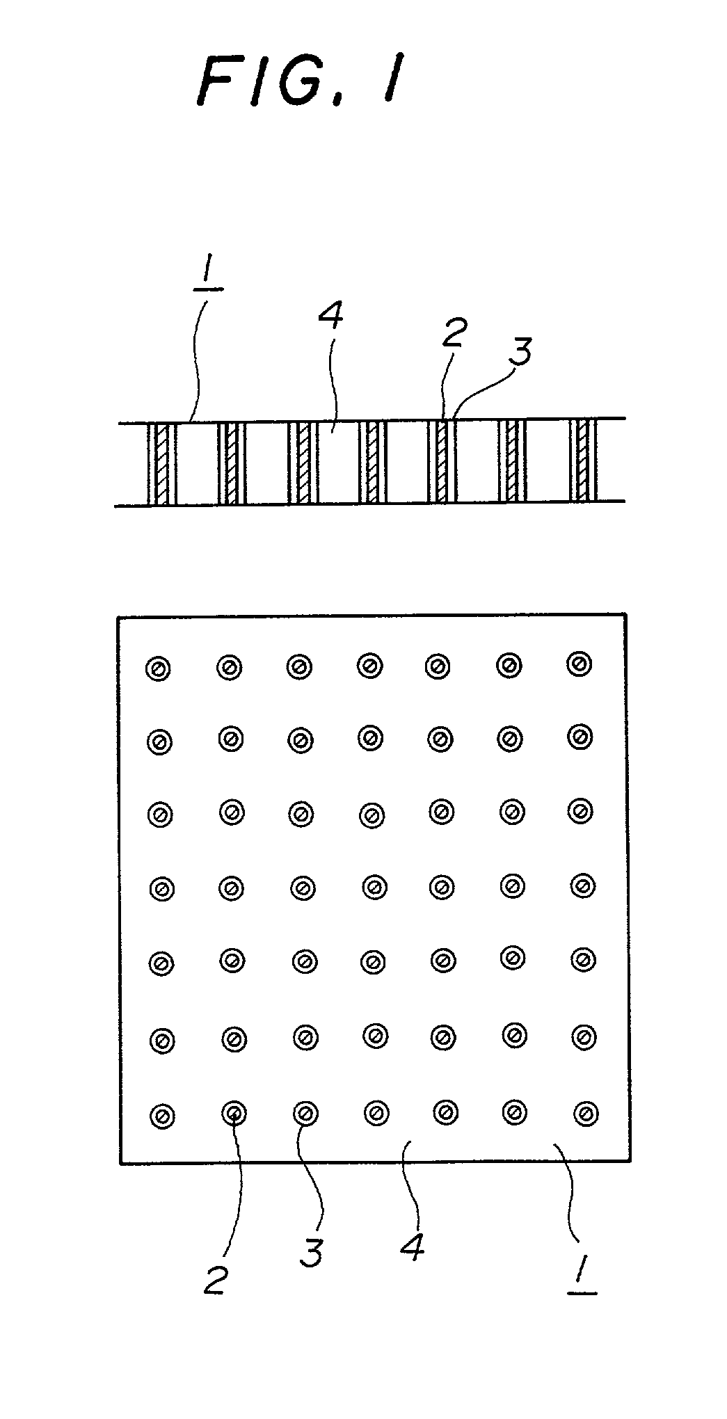
[0060]FIG. 1 shows lateral cross-sectional and plan views of a front-and-back electrically conductive substrate according to a first embodiment of the present invention (hereinafter the first front-and-back electrically conductive substrate). Reference numeral 1 indicates a front-and-back electrically conductive substrate, reference numeral 2 indicates a post, and reference numeral 3 indicates an electrically conductive portion consisting of an electrically conductive film covering a vicinity of a post. The electrically conductive film may be selected as appropriate from among metals such as tungsten, molybdenum, platinum, gold, copper and the like, so long as the metal selected is an electrically conductive metal having a melting point that is higher than the baking temperature of a ceramic-type insulating material to be described later. Reference numeral 4 indicates an insul...

second embodiment

[0084]A description will now be given of a front-and-back electrically conductive substrate according to the present invention, with reference to FIGS. 6, 7 and 8 (hereinafter second front-and-back electrically conductive substrate).

[0085]The second front-and-back electrically conductive substrate is the same as the first front-and-back electrically conductive substrate described above, with the addition of anti-noise measures. The effective use of co-axial cable as an anti-noise measure is widely known. In other words, in a construction consisting of a wire core, insulating material wrapped around the wire core and a metallic coating that wraps around the insulating material, adjusting the dielectric constant of the insulation as well as the distance from the core wire to the metallic coating makes it possible to create a noise-resistant structure.

[0086]The second front-and-back electrically conductive substrate represents the application of the above-described thinking to through ...

third embodiment

[0100]A description will now be given of a front-and-back electrically conductive substrate according to the present invention, with reference to FIGS. 9 and 10 (hereinafter the third front-and-back electrically conductive substrate).

[0101]FIG. 9 is a first diagram showing lateral and plan views of a front-and-back electrically conductive substrate according to a third embodiment of the present invention. FIG. 10 is a second diagram showing lateral and plan views of a front-and-back electrically conductive substrate according to a third embodiment of the present invention. As can be appreciated, both diagrams show that the third front-and-back electrically conductive substrate is a substrate that, like the second front-and-back electrically conductive substrate, employs a coaxial through hole construction, essentially a variation of the through hole construction shown in the second front-and-back electrically conductive substrate.

[0102]The coaxial through holes formed in the second ...


PUM

PropertyMeasurementUnit
aspect ratiosaaaaaaaaaa
heightsaaaaaaaaaa

Abstract

A front-and-back electrically conductive substrate includes a plurality of posts composed of a material that can be anisotropically etched and having an electrically conductive portion that has at least a first surface and a second surface that communicate with each other, and an insulative substrate that supports the plurality of posts.

Description

BACKGROUND OF THE INVENTION[0001]1. Field of the Invention[0002]The present invention relates generally to a front-and-back electrically conductive substrate and a method for manufacturing same, and more particularly, to a high-density front-and-back electrically conductive substrate capable of adapting to the high integration density, increasing post numbers and compactness of the LSIs required for electronic calculators and the like.[0003]2. Description of Related Art[0004]In recent years, the LSI packages and printed wiring boards have needed to acquire ever greater densities as the LSIs and other semiconductor components have become more highly integrated and equipped with a larger number of posts.[0005]With the LSI packages, the LSI chip is mounted face down on a ceramic substrate or an organic substrate. Further, the ceramic substrate or organic substrate is mounted on a printed wiring board using balls of solder.[0006]In order to obtain an electrical conduction between a firs...

Claims


Application Information

Patent Timeline
Patent Type & Authority Patents(United States)
IPC IPC(8): H05K1/16H01L21/48H01L23/12H01L23/15H01L23/48H01L23/498H05K1/02H05K1/11H05K3/06H05K3/40H05K3/46
CPCH01L21/486H01L23/49822H01L23/49827H01L23/49833H05K1/0222H05K3/4038H05K3/4602H01L23/481H01L23/147Y10T29/49204H01L2223/6622H01L2924/01078H01L2924/01079H01L2924/09701H01L2924/15311H01L2924/15312H01L2924/3011H05K1/115H05K3/06H05K2201/09809H05K2203/0369H01L2224/73204H01L2924/10253Y10T29/49126H01L2224/16235Y10T29/49165Y10T29/49155Y10T29/49222H01L2924/00H01L2924/00014H01L2224/0401
Inventor MORIIZUMI, KIYOKAZU
Owner FUJITSU LTD
Why Eureka
Try Eureka