Semiconductor memory device comprising one or more injecting bilayer electrodes

a memory device and bilayer electrode technology, applied in thermoelectric devices, instruments, nanoinformatics, etc., can solve the problems of increasing complexity of components, increasing power consumption and efficiency of components, and generally not being able to retain information stored or programmed within, etc., to facilitate the formation of such memory devices, facilitate significant improvement of electron injection, and facilitate significant improvement of hole injection

Active Publication Date: 2009-09-01
MONTEREY RES LLC
View PDF5 Cites 7 Cited by
  • Summary
  • Abstract
  • Description
  • Claims
  • Application Information

AI Technical Summary

Benefits of technology

[0007]The subject invention relates generally to semiconductor devices and, in particular, to semiconductor memory devices comprising memory cells with one or more injecting bilayer electrodes. The invention provides for systems and methods that facilitate forming such memory devices. Modern memory arrays typically comprise bit cells that have two discrete components, a memory element and a selection element, such as, for example, a diode. In accordance with one aspect of the invention, a memory cell is formed comprising a bilayer cathode that facilitates a significant improvement in electron injection into the diode layers of selected memory cells. Similarly, in accordance with another aspect of the invention, a memory cell is formed comprising a bilayer anode that facilitates a significant improvement in hole injection into the diode layers of selected memory cells. In accordance with another aspect of the invention, the increased charge (e.g. electrons or holes) density in the diode layers of the selected memory cells results in improved memory cell switching times and lowers the voltage required for the memory cell to operate, thereby, creating a more efficient memory cell.
[0008]According to another aspect of the invention, memory cells can be configured in a memory array such that the injecting bilayer electrodes are coupled to one of the control lines (e.g. word line or bit line). Furthermore, in accordance with another aspect of the invention, a memory array can be configured such that one of the control lines (e.g. word line or bit line) comprises the second layer of the injecting bilayer electrode and the memory cells comprise the first layer of the injecting bilayer electrodes. Further, in accordance with yet another aspect of the invention, a memory array can be configured such that one of the control lines (e.g. word line or bit line) comprises both the first and second layers of the injecting bilayer electrodes and couple directly to the diode layer of the memory cell. In accordance with another aspect of the invention, memory arrays formed from memory cells comprising selection diodes with injecting bilayer electrode(s) will have increased charge density in the diode layers of the selected memory cells. The increased charge density resulting from the injecting bilayer electrodes results in improved memory cell switching times and lower required operational voltage, thereby, creating a more efficient memory array.

Problems solved by technology

Volatile memory components generally cannot retain information stored or programmed within them when the component loses power.
As components increase in complexity, power consumption and efficiency of the components becomes more critical.

Method used


Image

  • Semiconductor memory device comprising one or more injecting bilayer electrodes
  • Semiconductor memory device comprising one or more injecting bilayer electrodes
  • Semiconductor memory device comprising one or more injecting bilayer electrodes

Examples


Embodiment Construction

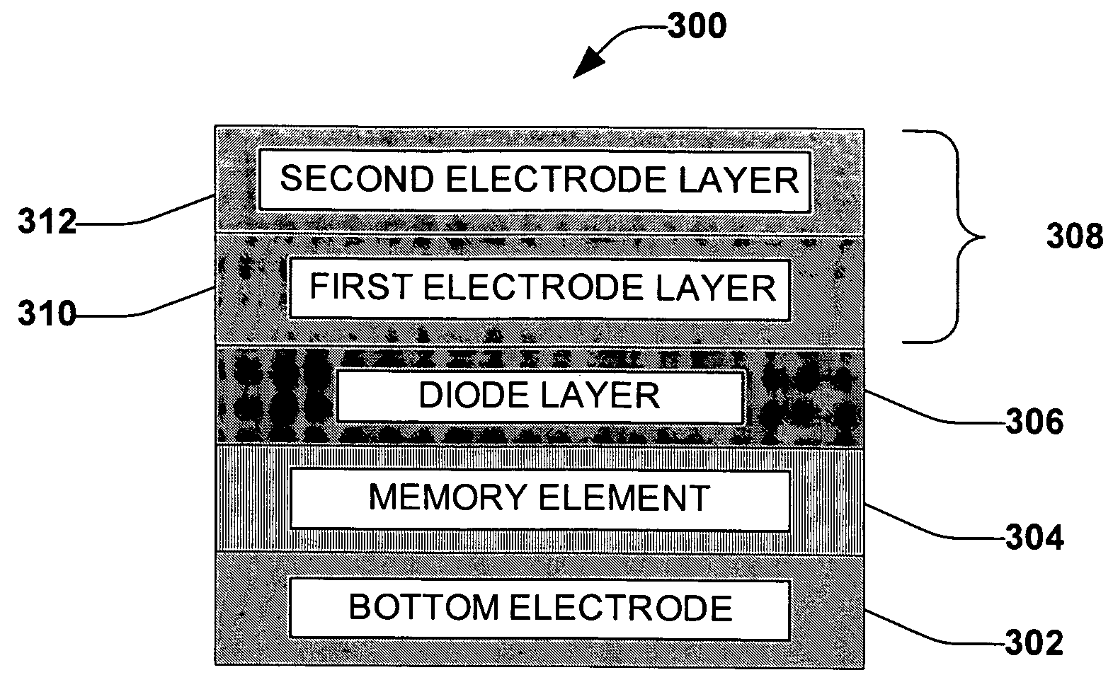
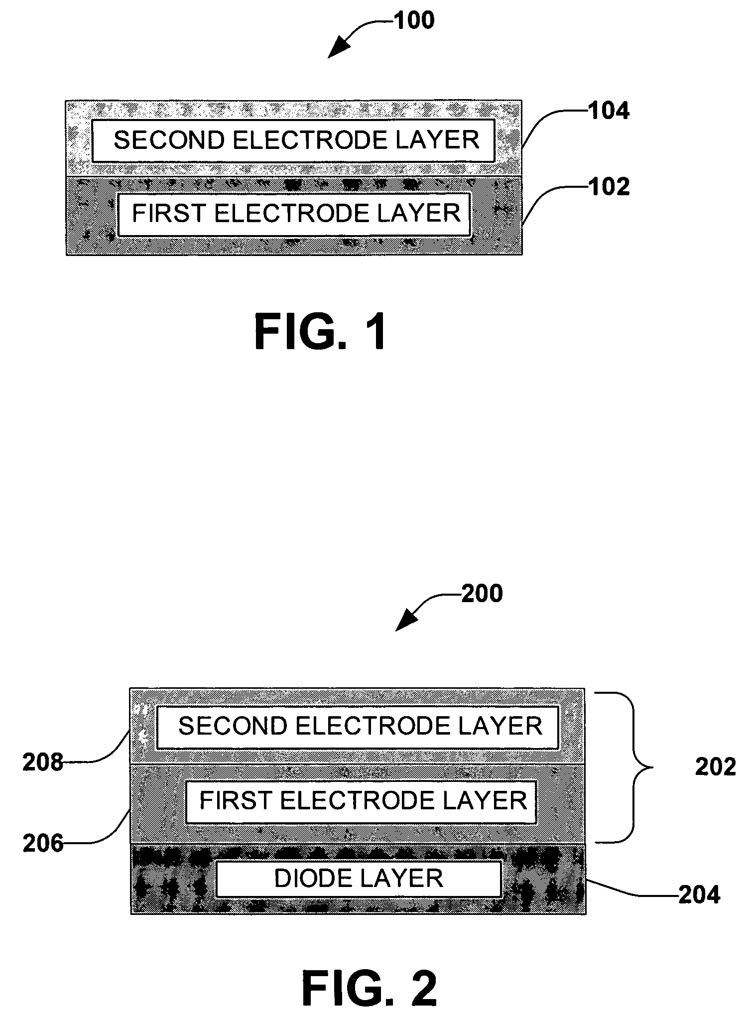
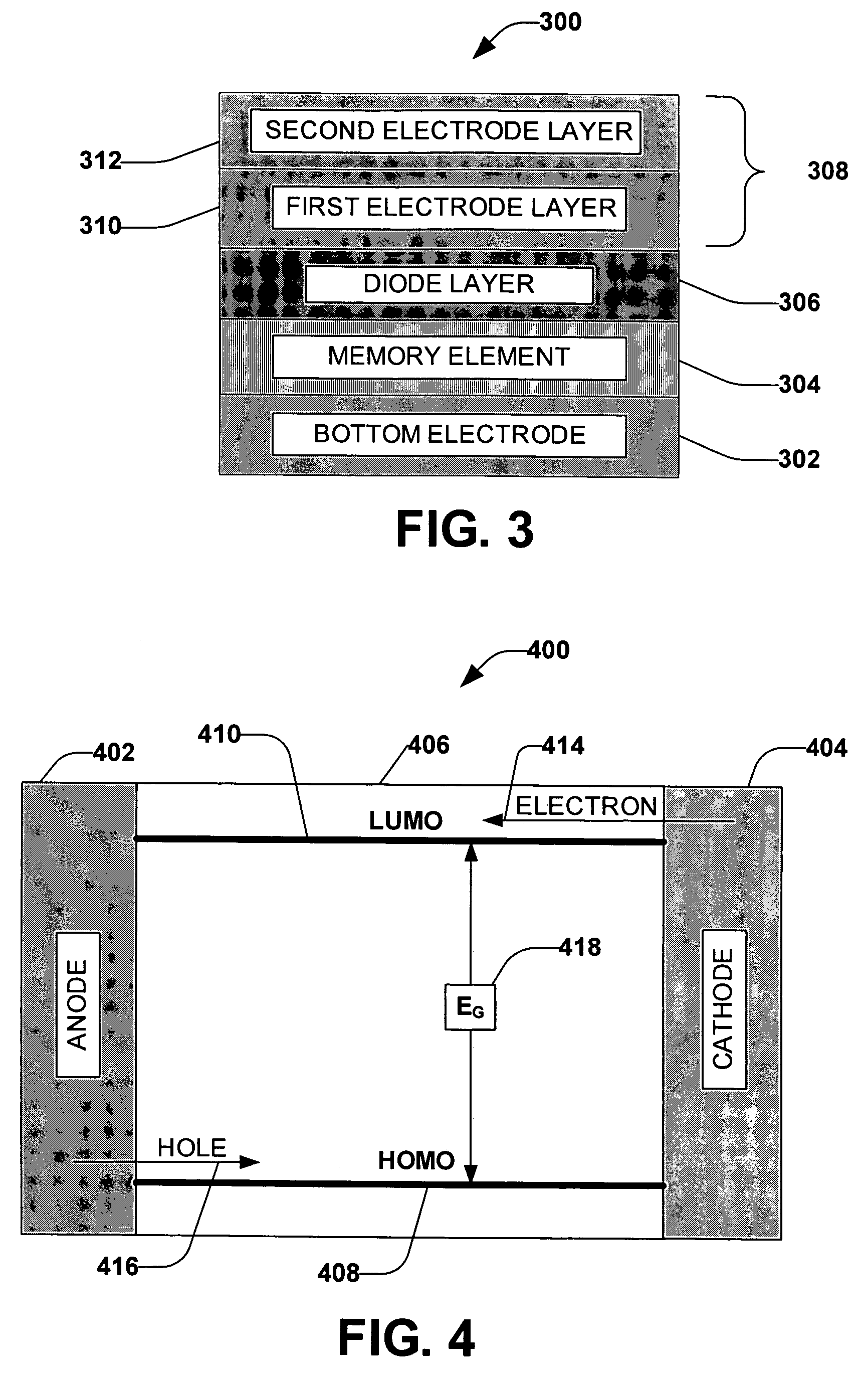
[0019]The invention will now be described with reference to the drawings, wherein like reference numerals are used to refer to like elements throughout. The invention will be described with reference to systems and methods that facilitate providing a memory device comprising a bilayer electrode that enhances charge injection into a polymer layer of a diode. It should be understood that the description of these exemplary aspects are merely illustrative and that they should not be taken in a limiting sense.

[0020]The term “component” can refer to a computer-related entity, either hardware, a combination of hardware and software, software, or software in execution. For example, a component can be a process running on a processor, a processor, an object, an executable, a thread of execution, a program and a computer. By way of illustration, both an application running on a server and the server can be components. A component can reside in one physical location (e.g., in one computer) and...


PUM


Abstract

The subject invention provides systems and methods that facilitate formation of semiconductor memory devices comprising memory cells with one or more injecting bilayer electrodes. Memory arrays generally comprise bit cells that have two discrete components; a memory element and a selection element, such as, for example, a diode. The invention increases the efficiency of a memory device by forming memory cells with selection diodes comprising a bilayer electrode. Memory cells are provided comprising bilayer cathodes and / or bilayer anodes that facilitate a significant improvement in charge injection into the diode layers of memory cells. The increased charge (e.g. electrons or holes) density in the diode layers of the selected memory cells results in improved memory cell switching times and lowers the voltage required for the memory cell to operate, thereby, creating a more efficient memory cell.

Description

FIELD OF INVENTION[0001]The subject invention relates generally to semiconductor devices and, in particular, to semiconductor memory devices comprising memory cells with one or more injecting bilayer electrodes.BACKGROUND OF THE INVENTION[0002]The reduction in size of semiconductor components and increased usage of semiconductor processors has lead to an explosion of new electronic devices. Most, if not all, of these electronic devices require some amount of memory in order to function. The proliferation of such devices has significantly increased demand for memory that is efficient in size as well as power consumption. Smaller sized semiconductor components and memories have made numerous hand held electronic devices feasible. Examples of hand-held devices include cell phones, personal radios, walkie-talkies, personal data assistants, palm pilots, pagers, notebook computers, remote controls, voice recorders, audio recorders, video recorders, radios, small televisions, web viewers, ...

Claims


Application Information

Patent Timeline
Patent Type & Authority Patents(United States)
IPC IPC(8): H01L29/08
CPCB82Y10/00G11C13/0014G11C13/0016H01L27/285G11C2213/56G11C2213/71G11C2213/72G11C2213/55H10K19/202
Inventor SOKOLIK, IGORKINGSBOROUGH, RICHARD P.MANDELL, AARON
Owner MONTEREY RES LLC
Why Eureka
Try Eureka