Field emission device and method for making the same

a field emission device and field technology, applied in the manufacture of electric discharge tubes/lamps, electrode systems, discharge tubes luminescnet screens, etc., can solve the problems of time-consuming and difficult to operate mechanical means, need high emission voltages to emit electrons, and inability to carry high electric current reliably

Active Publication Date: 2009-09-08
BEIJING FUNATE INNOVATION TECH +1
View PDF6 Cites 17 Cited by
  • Summary
  • Abstract
  • Description
  • Claims
  • Application Information

AI Technical Summary

Benefits of technology

[0005]Carbon nanotube-based field emission devices typically include a base acting as a cathode plate, and a carbon nanotube array acting as an emitter formed on the base. Methods for forming the carbon nanotube array on the base typically include mechanical means and in situ growth. The mechanical means consists of fixing carbon nanotubes onto the base with chemical agglutinant using a robot arm. Such a mechanical means is time consuming and difficult to operate. Furthermore, it is impossible to manipulate the carbon nanotubes with a diameter smaller than about 1 nm (nanometer).

Problems solved by technology

However, such materials need high emission voltages to emit electrons, and cannot carry high electric current reliably.
Such a mechanical means is time consuming and difficult to operate.
Furthermore, it is impossible to manipulate the carbon nanotubes with a diameter smaller than about 1 nm (nanometer).
Secondly, a carbon nanotube array is grown on the base by a chemical vapor deposition (CVD) process.
However, the carbon nanotube array is generally fabricated under a temperature in the range from 500 to 900° C. As a result, the driving circuit on the base may be damaged.

Method used


Image

  • Field emission device and method for making the same
  • Field emission device and method for making the same
  • Field emission device and method for making the same

Examples


Embodiment Construction

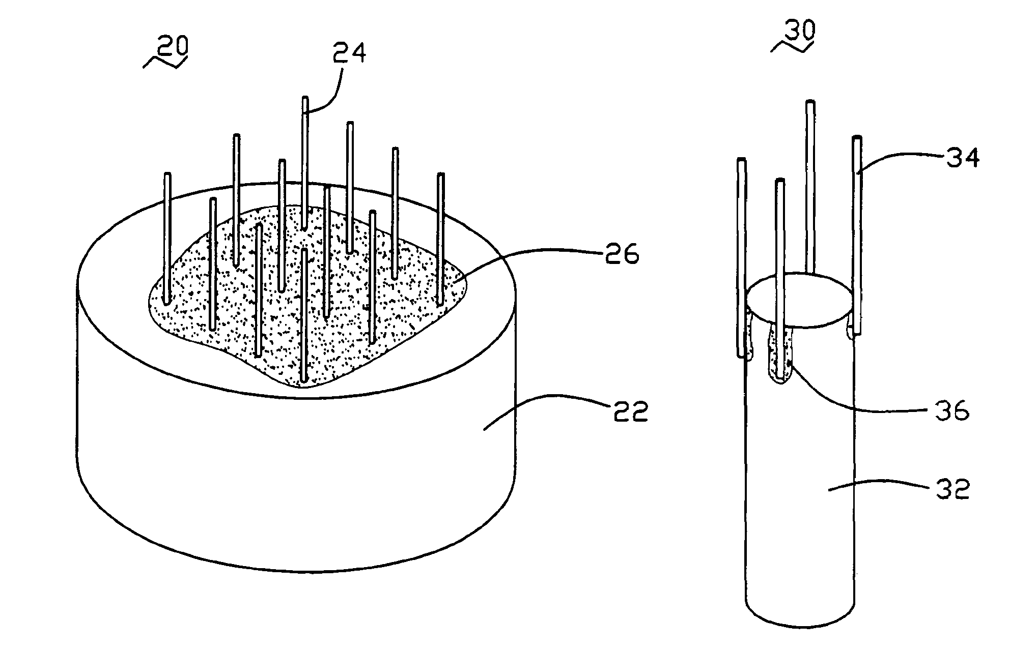
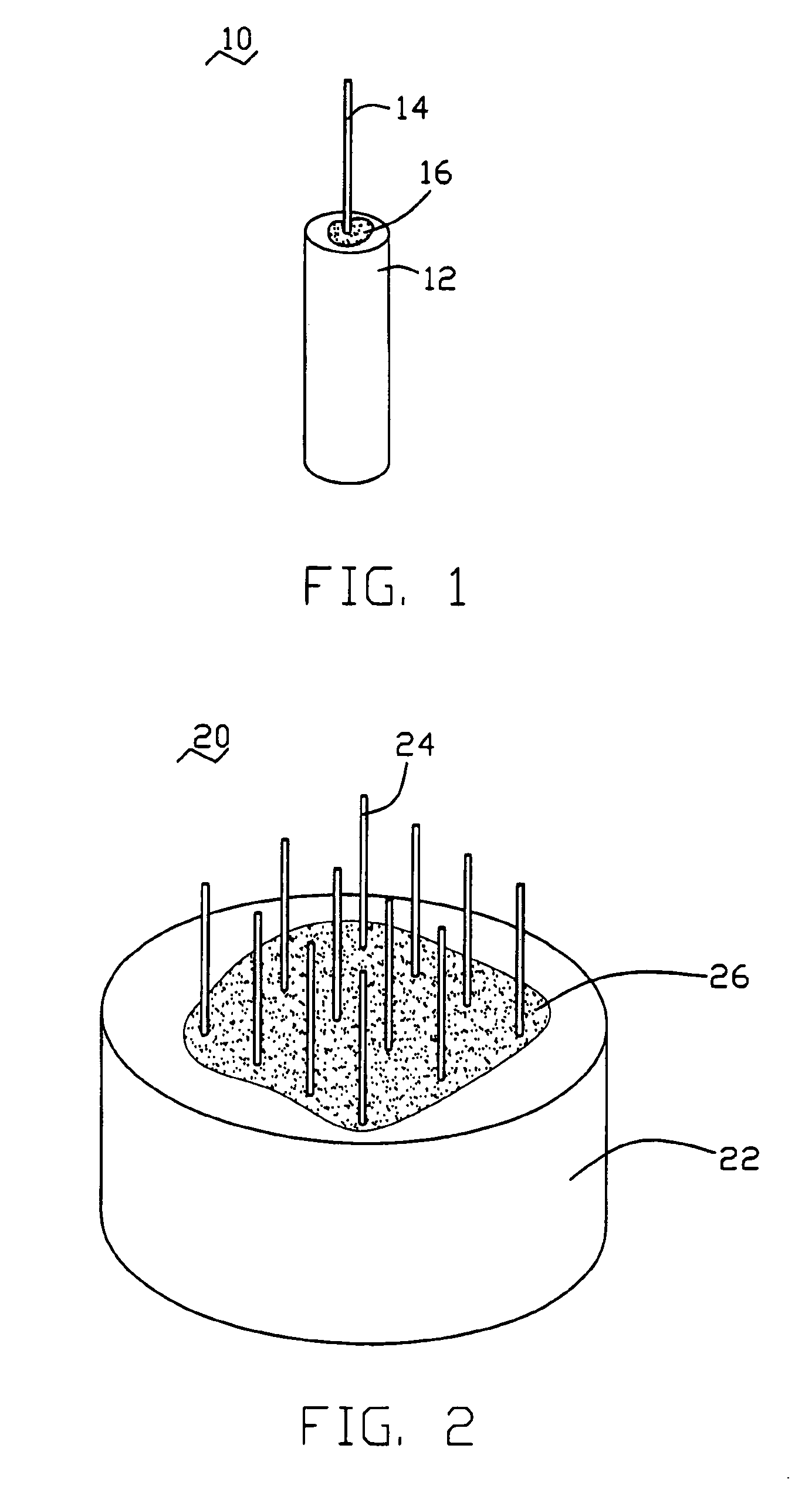
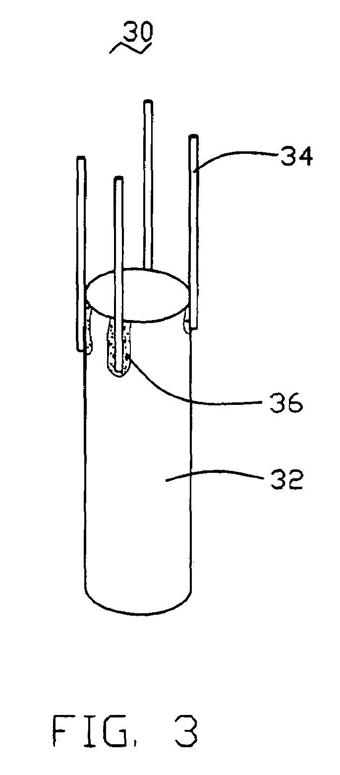
[0017]Reference will now be made to the drawings to describe in detail the preferred embodiments of the present field emission device and a method for making thereof.

[0018]In order to improve manipulability, macroscopic carbon nanotube structures are proposed for use as emitters in the present embodiment. Assembling carbon nanotubes into macroscopic structures is of great importance to their applications at the macroscopic level.

[0019]That a long macroscopic carbon nanotube yarn can be drawn out from a superaligned carbon nanotube array has been disclosed in US Pub. No. 20040053780, which is incorporated herein by reference. A carbon nanotube yarn includes a plurality of carbon nanotube bundles that are joined end to end by van der Waals attractive force, and each of the carbon nanotube bundles includes a plurality of carbon nanotubes substantially parallel to each other. Each carbon nanotube bundle is joined with the carbon nanotubes adjacent to it at either end in a sideward direc...


PUM


Abstract

A field emission device (10) includes a base (12), a conductive paste (16), and at least one carbon nanotube yarn (14). The at least one carbon nanotube yarn is attached to the base using the conductive paste. This avoids separation of the at least one carbon nanotube yarn from the base by electric field force in a strong electric field. A method for making the field emission device includes the steps of: (a) providing a base; (b) attaching at least one carbon nanotube yarn to the base using conductive paste; and (c) sintering the conductive paste to obtain the field emission device with the carbon nanotube yarn firmly attached to the base.

Description

BACKGROUND[0001]1. Technical Field[0002]The present invention relates to field emission devices, and particularly to a field emission device using carbon nanotube yarns as emitters and method for making the field emission device.[0003]2. Discussion of Related Art[0004]Field emission materials are used in a variety of application such as flat panel displays to emit electrons. Typical field emission materials include, for example, molybdenum (Mo), tantalum (Ta), silicon (Si), and diamond. However, such materials need high emission voltages to emit electrons, and cannot carry high electric current reliably. Carbon nanotubes typically have superior performance including, in particular, good electron emission capability at low emission voltages, generally less than 100 volts. Furthermore, carbon nanotubes can carry high electric current reliably Due to these properties, carbon nanotubes are considered to be an ideal field emission material for a variety of applications, especially in fie...

Claims


Application Information

Patent Timeline
Patent Type & Authority Patents(United States)
IPC IPC(8): H01J9/02
CPCH01J9/025H01J1/304Y10S977/842Y10S977/882
Inventor JIANG, KAI-LIWEI, YANGLIU, PENGLIU, LIANGFAN, SHOU-SHAN
Owner BEIJING FUNATE INNOVATION TECH
Why Eureka
Try Eureka