Semiconductor device having well with peak impurity concentrations and method for fabricating the same

a semiconductor and impurity concentration technology, applied in the direction of semiconductor devices, basic electric elements, electrical appliances, etc., can solve the problem of difficult control of the threshold voltage by the substrate bias, and achieve the effect of increasing the gate charge quantity, reducing the scattering of dopant ions, and increasing the carrier mobility

Inactive Publication Date: 2009-09-22
SOCIONEXT INC
View PDF11 Cites 109 Cited by
  • Summary
  • Abstract
  • Description
  • Claims
  • Application Information

AI Technical Summary

Benefits of technology

[0010]An object of the present invention is to provide a semiconductor device of high performance which permits even a downsized MIS transistor to control the threshold voltage by the substrate bias, and a method for fabricating the semiconductor device.
[0016]The well including an impurity diffused region having a peak of an impurity concentration in a region deeper than the pocket region, and the threshold voltage of the transistor is controlled by this impurity diffused region, whereby the impurity concentration near the surface side of the channel region can be decreased in comparison with the case that the impurity diffused region for the threshold voltage control is formed in region shallower than the pocket region. Accordingly, the carrier scattering by the dopant ions is decreased, and the carrier mobility can be increased.

Problems solved by technology

Especially in much downsized MIS transistors whose gate length is below, e.g., 60 nm, it is difficult to control the threshold voltage by the substrate bias.

Method used


Image

  • Semiconductor device having well with peak impurity concentrations and method for fabricating the same
  • Semiconductor device having well with peak impurity concentrations and method for fabricating the same
  • Semiconductor device having well with peak impurity concentrations and method for fabricating the same

Examples


Embodiment Construction

[0026]The semiconductor device and the method for fabricating the same according to one embodiment of the present invention will be explained with reference to FIGS. 1 to 12B.

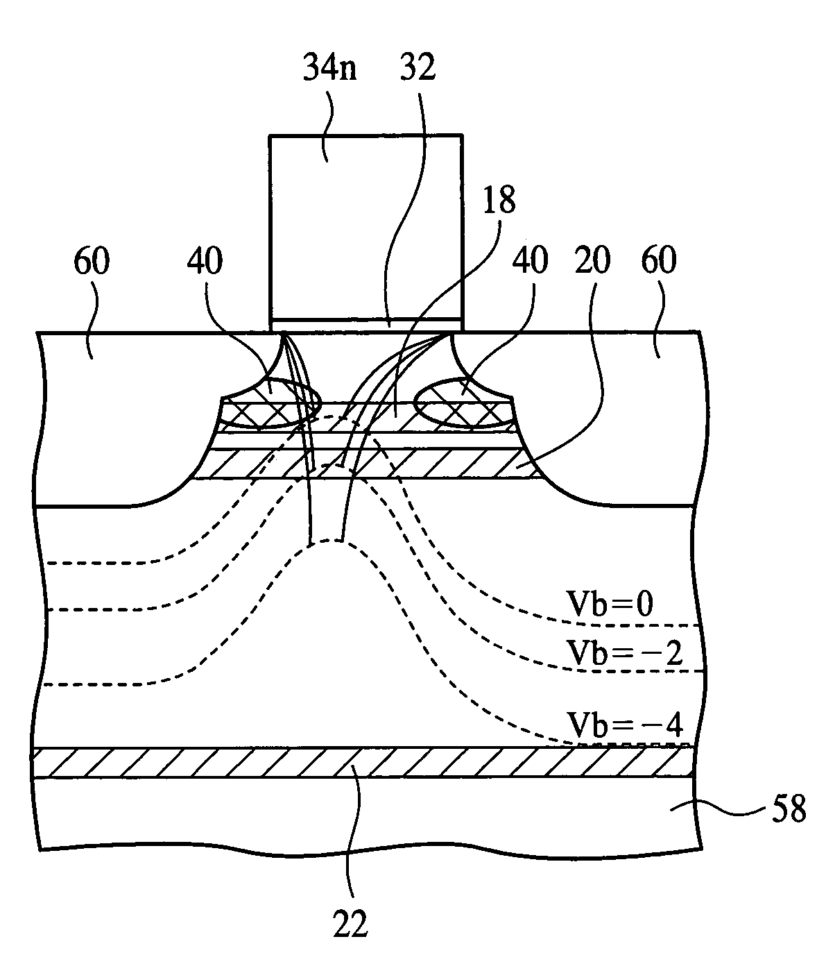
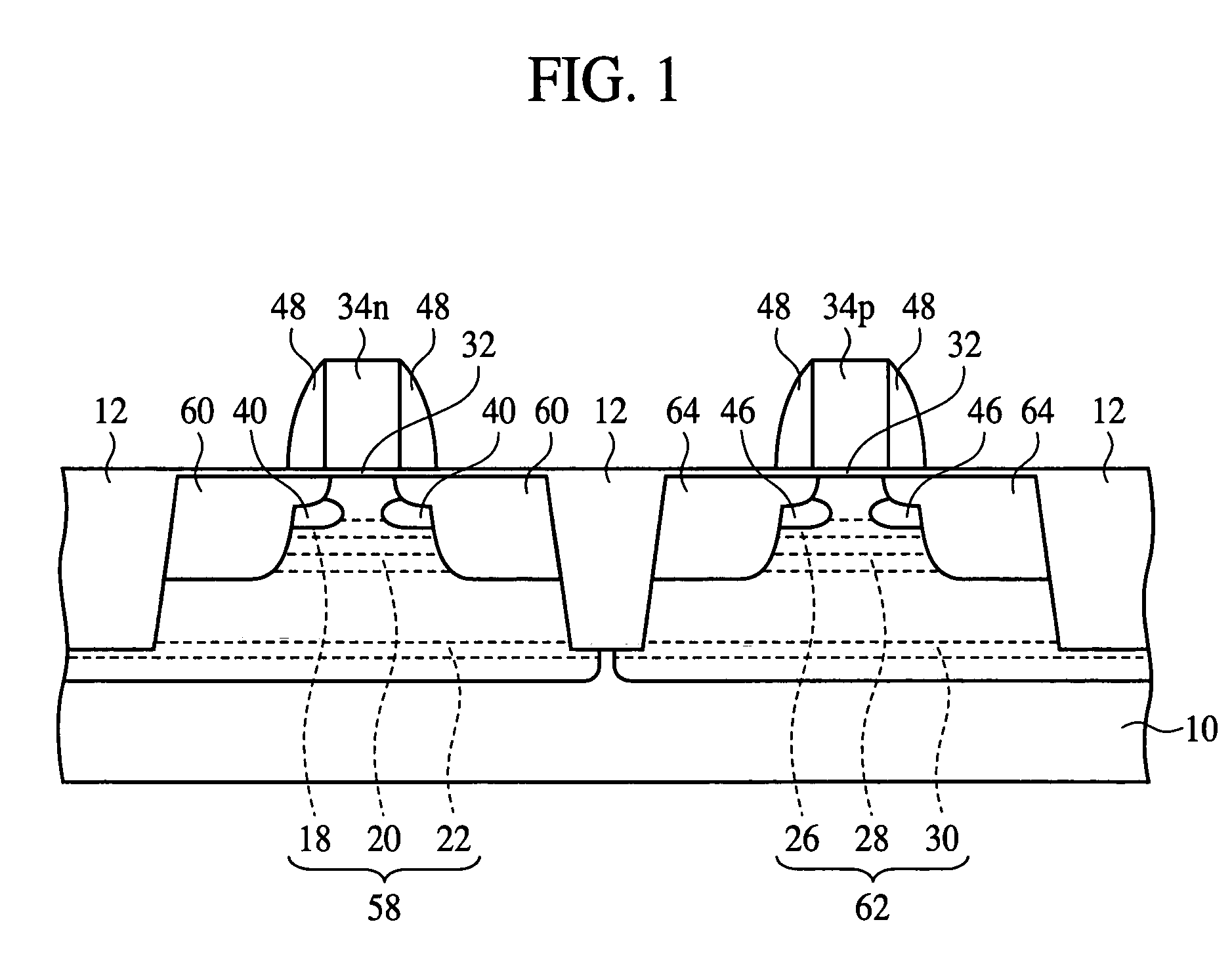
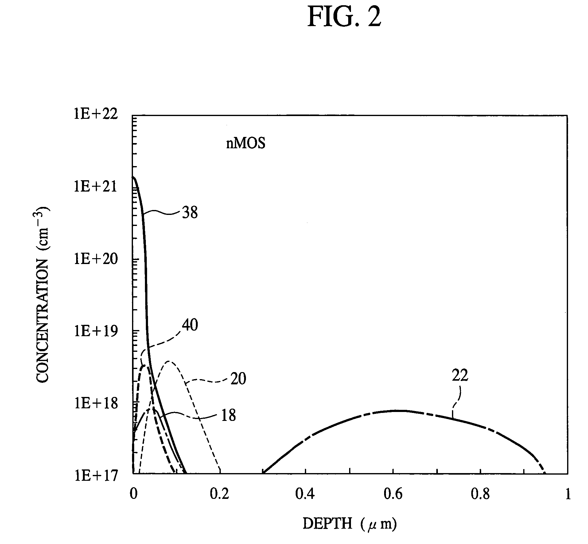
[0027]FIG. 1 is a diagrammatic sectional view of the semiconductor device according to the present embodiment, which shows a structure thereof. FIGS. 2 and 3 are graphs of impurity concentration distributions in the silicon substrate of the semiconductor device according to the present embodiment. FIG. 4 is a diagrammatic sectional view of a general semiconductor device, which shows the structure thereof. FIGS. 5A and 5B are graphs of substrate bias dependency of the Id-Vg characteristics of the semiconductor device shown in FIG. 4. FIGS. 6A and 6B are diagrammatic views of the positions of the ends of the depletion layers and the range of the ends of the electric flux lines from the gate electrode in the semiconductor device shown in FIG. 4. FIG. 7 is a diagrammatic view of the positions of the ends of the dep...


PUM


Abstract

The semiconductor device comprises a well 58 formed in a semiconductor substrate 10 and having a channel region; a gate electrode 34n formed over the channel region with an insulating film 32 interposed therebetween; source / drain regions 60 formed in the well 58 on both sides of the gate electrode 34n, sandwiching the channel region; and a pocket region 40 formed between the source / drain region and the channel region. The well 58 has a first peak of an impurity concentration at a depth deeper than the pocket region 40 and shallower than the bottom of the source / drain regions 60, and a second peak of the impurity concentration at a depth near the bottom of the source / drain regions 60.

Description

CROSS-REFERENCE TO RELATED APPLICATIONS[0001]This application is based upon and claims the benefit of priority from the prior Japanese Patent Application No. 2004-278870, filed on Sep. 27, 2004, the entire contents of which are incorporated herein by reference.BACKGROUND OF THE INVENTION[0002]The present invention relates to a semiconductor device and a method for fabricating the same, more specifically, a semiconductor device including MIS transistor in which the threshold voltage is controlled by a substrate bias, and a method for fabricating the semiconductor device.[0003]As semiconductor device is more downsized and higher integrated, MIS transistor is required to be more speedy and have lower operation voltages.[0004]For higher speed of a MIS transistor, it is effective to constitute the MIS transistor to have a low threshold voltage and make a drive voltage to be applied to the drain higher. That is, the drive force of the MIS transistor depends on a voltage difference between...

Claims


Application Information

Patent Timeline
Patent Type & Authority Patents(United States)
IPC IPC(8): H01L21/425
CPCH01L21/823892H01L21/823807
Inventor TAKAO, YOSHIHIRO
Owner SOCIONEXT INC
Why Eureka
Try Eureka