

Semiconductor device and manufacturing method thereof
a technology of semiconductor and semiconductor components, applied in the field of semiconductor devices and manufacturing methods thereof, can solve the problems of low mobility of channel layers, high on-state resistance, and poor pinch-off characteristics of vertical fets disclosed in the first and second related arts, and achieve improved pinch-off characteristics, enhanced electron conduction layer mobility, and favorable electrical characteristics
- Summary
- Abstract
- Description
- Claims
- Application Information
AI Technical Summary
Benefits of technology
Problems solved by technology
Method used
Image

Examples
first embodiment
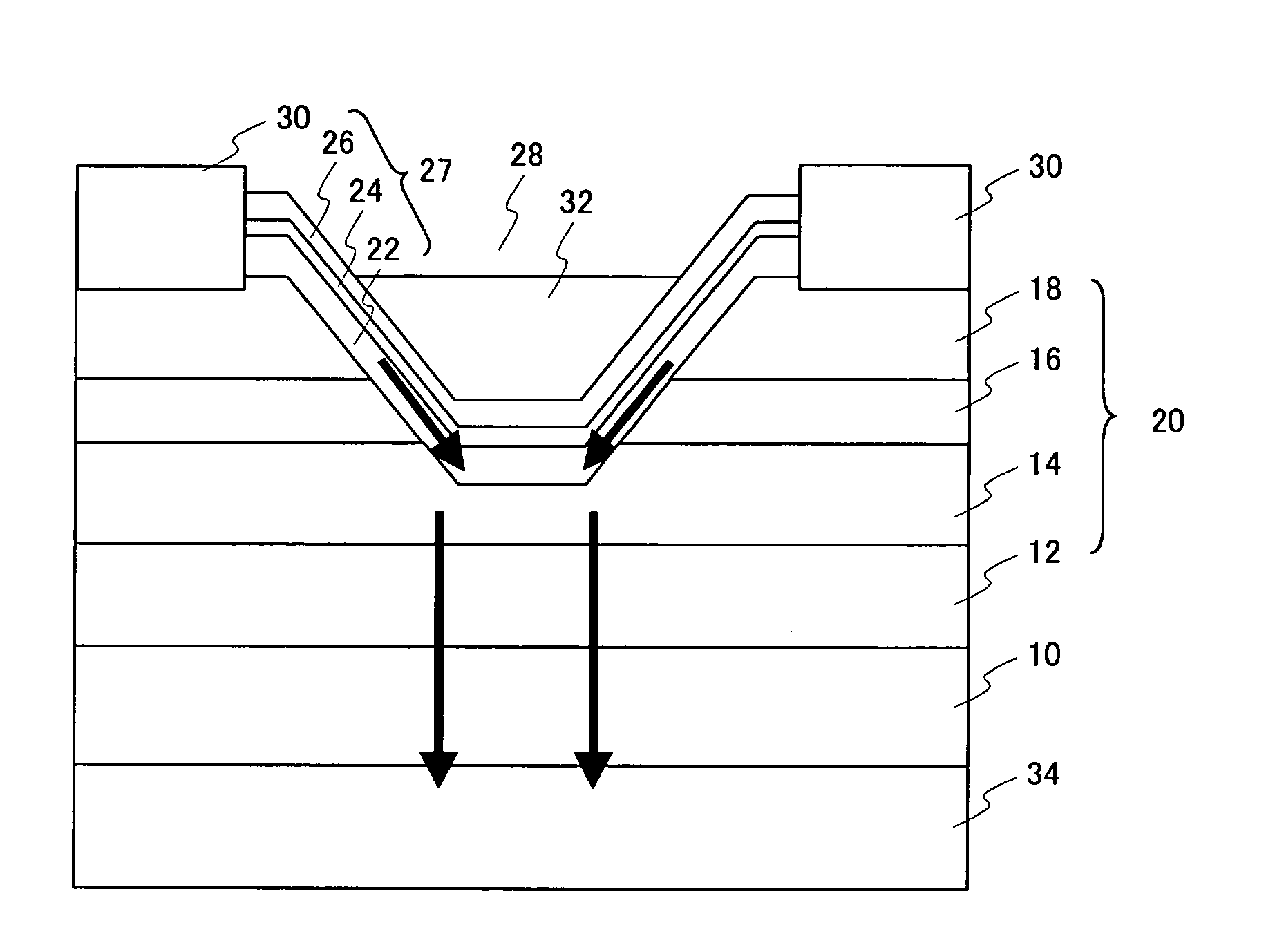
[0032]FIG. 3 is a cross-sectional view of a first embodiment. An N-type AlGaN buffer layer 12, an N-type GaN drift layer 14 (a first N-type GaN-based semiconductor layer), a P-type GaN or AlGaN barrier layer 16 (P-type GaN-based semiconductor layer) and an N-type GaN cap layer 18 (a second N-type GaN-based semiconductor layer) are formed on a conductive SiC substrate 10 in this order, as the GaN-based semiconductor layer 20. In other words, the GaN-based semiconductor layer 20 includes a P-type GaN-based semiconductor layer, and a first GaN-based semiconductor layer and a second semiconductor layer between which the P-type GaN-based semiconductor layer is sandwiched.
[0033]An opening region 28 that reaches the drift layer 14 is formed on the GaN-based semiconductor layer 20. In other words, at least the barrier layer 16 (P-type GaN-based semiconductor layer) is removed in the opening region 28. A GaN electron conduction layer 22 to which no impurities are added, an AlN intermediate l...
PUM
 Abstract
Description
Claims
Application Information