Method and device of measuring interface trap density in semiconductor device

a technology of interface trap density and semiconductor device, which is applied in the direction of semiconductor/solid-state device testing/measurement, instruments, testing circuits, etc., can solve the problems of degrading some characteristics of semiconductor devices, affecting the character of semiconductor devices, and deteriorating quality of gate oxide layer or driving current, etc., to achieve accurate measurement and calculation of interface trap density

Inactive Publication Date: 2009-09-22
DONGBU ELECTRONICS CO LTD
View PDF3 Cites 19 Cited by
  • Summary
  • Abstract
  • Description
  • Claims
  • Application Information

AI Technical Summary

Benefits of technology

[0009]An object of the present invention is to more accurately measure and calculate interface trap density in a semiconductor device having a thin gate oxide layer.

Problems solved by technology

Accordingly, characteristics of semiconductor devices are inevitably affected by these smaller dimensions.
Accordingly, the quality of the gate oxide layer deteriorates or the driving current is reduced, which may degrade some characteristics of a semiconductor device.
However, when the conventional method is applied to a device having a very thin gate oxide layer, gate tunneling leakage current and / or quantum mechanical effects can result in an incorrect calculation of the interface trap density (generally resulting in a calculated interface trap density that is too high).

Method used


Image

  • Method and device of measuring interface trap density in semiconductor device
  • Method and device of measuring interface trap density in semiconductor device
  • Method and device of measuring interface trap density in semiconductor device

Examples


Embodiment Construction

[0018]Reference will now be made in detail to the preferred embodiments of the present invention, examples of which are illustrated in the accompanying drawings.

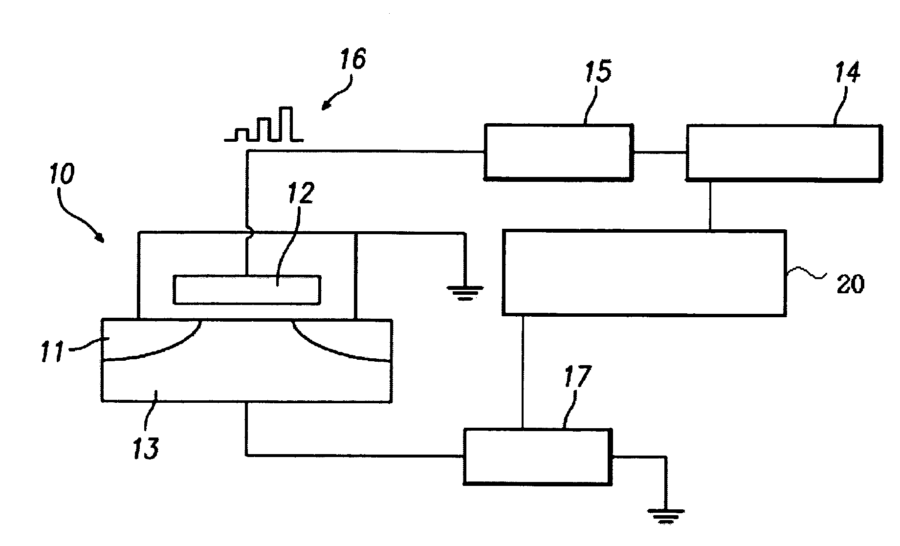
[0019]FIG. 1 is a view illustrating a construction of an apparatus for measuring a charge pumping current according to an embodiment of the present invention.

[0020]Referring to FIG. 1, a pulse 16 having a fixed base voltage is applied to a gate 12 of a transistor in wafer 10, with source / drain 11 of the transistor grounded, and an amperemeter 17 in a measuring apparatus connected to a bulk 13 (also called a body or a base) of the transistor. Accordingly, a gate channel of the transistor operates between an accumulation state and an inversion state to generate the charge pumping current (Icp) This current is measured from the bulk 13 (e.g. by amperemeter 17).

[0021]The pulse 16 has a fixed low level gate voltage (i.e., a base voltage) and an increasing high level gate voltage (i.e., a peak voltage). The pulse 16 is generated a...


PUM


Abstract

A method is provided for measuring interface trap density in a semiconductor device. In the method, measurement parameters are input to a host computer. A pulse condition is set at a pulse generator using the measurement parameters. A pulse of a predetermined frequency generated by the pulse generator is applied to a gate of a transistor, and a charge pumping current is measured from a bulk of the transistor. A charge pumping current measurement may be repeated for a plurality of frequencies while changing the frequency until a set frequency is reached. A pure charge pumping current is calculated for each frequency where a gate tunneling leakage current is removed from the charge pumping current measured for each frequency. Interface trap density is calculated from the calculated pure charge pumping current for each frequency.

Description

BACKGROUND OF THE INVENTION[0001]1. Field of the Invention[0002]The present invention relates to a method and device for measuring interface trap density in a semiconductor device.[0003]2. Description of the Related Art[0004]As a semiconductor technology develops constantly, the length of gates gradually become shorter and the thickness of gate oxide layers gradually become thinner. Accordingly, characteristics of semiconductor devices are inevitably affected by these smaller dimensions. One of the characteristics affected is the interface trap density between a silicon substrate and a gate oxide layer.[0005]Generally, when a gate oxide layer is grown, a sufficient bonding is not made between a silicon atom and an oxygen atom, so that a dangling bond (where there are insufficient oxygen atoms) is generated at an interface between a silicon substrate and the gate oxide layer.[0006]A dangling bond easily attracts an electron when a transistor operates, thereby increasing the interface...

Claims


Application Information

Patent Timeline
Patent Type & Authority Patents(United States)
IPC IPC(8): G01R31/28G06F19/00H01L21/66
CPCG01R31/2648H01L22/00
Inventor SONG, JONG KYU
Owner DONGBU ELECTRONICS CO LTD
Why Eureka
Try Eureka