Memory cell comprising a molecular transistor, device comprising a plurality of such cells and method for using same

a molecular transistor and memory cell technology, applied in read-only memories, static storage, instruments, etc., can solve the problems of difficult access to data contained in predetermined memory transistors without, cell however only operating correctly, etc., to increase the interconnection density, simple production, reliable data access

Inactive Publication Date: 2009-09-22
COMMISSARIAT A LENERGIE ATOMIQUE ET AUX ENERGIES ALTERNATIVES
View PDF8 Cites 0 Cited by
  • Summary
  • Abstract
  • Description
  • Claims
  • Application Information

AI Technical Summary

Benefits of technology

[0010]It is one object of the invention to provide a memory cell that is simple to produce and reliable for data access without deleting the data of another cell when read is performed, while providing a compact cell, to increase the interconnection density, and multivalued, i.e. a cell enabling several values to be stored on a single memory dot. The cell is selectable, i.e. it enables selective access to particular data without damaging the data contained in the other cells, in particular the neighboring cells.

Problems solved by technology

When such a memory transistor is integrated in a memory device organized in lines and columns, it is difficult to access the data contained in a predetermined transistor of the memory without disturbing the other transistors and / or without being disturbed by the signals from the other transistors connected to the same access conductors.
Such a cell however only operates correctly when two types of molecules are used for the memory transistor.

Method used


Image

  • Memory cell comprising a molecular transistor, device comprising a plurality of such cells and method for using same
  • Memory cell comprising a molecular transistor, device comprising a plurality of such cells and method for using same
  • Memory cell comprising a molecular transistor, device comprising a plurality of such cells and method for using same

Examples


Embodiment Construction

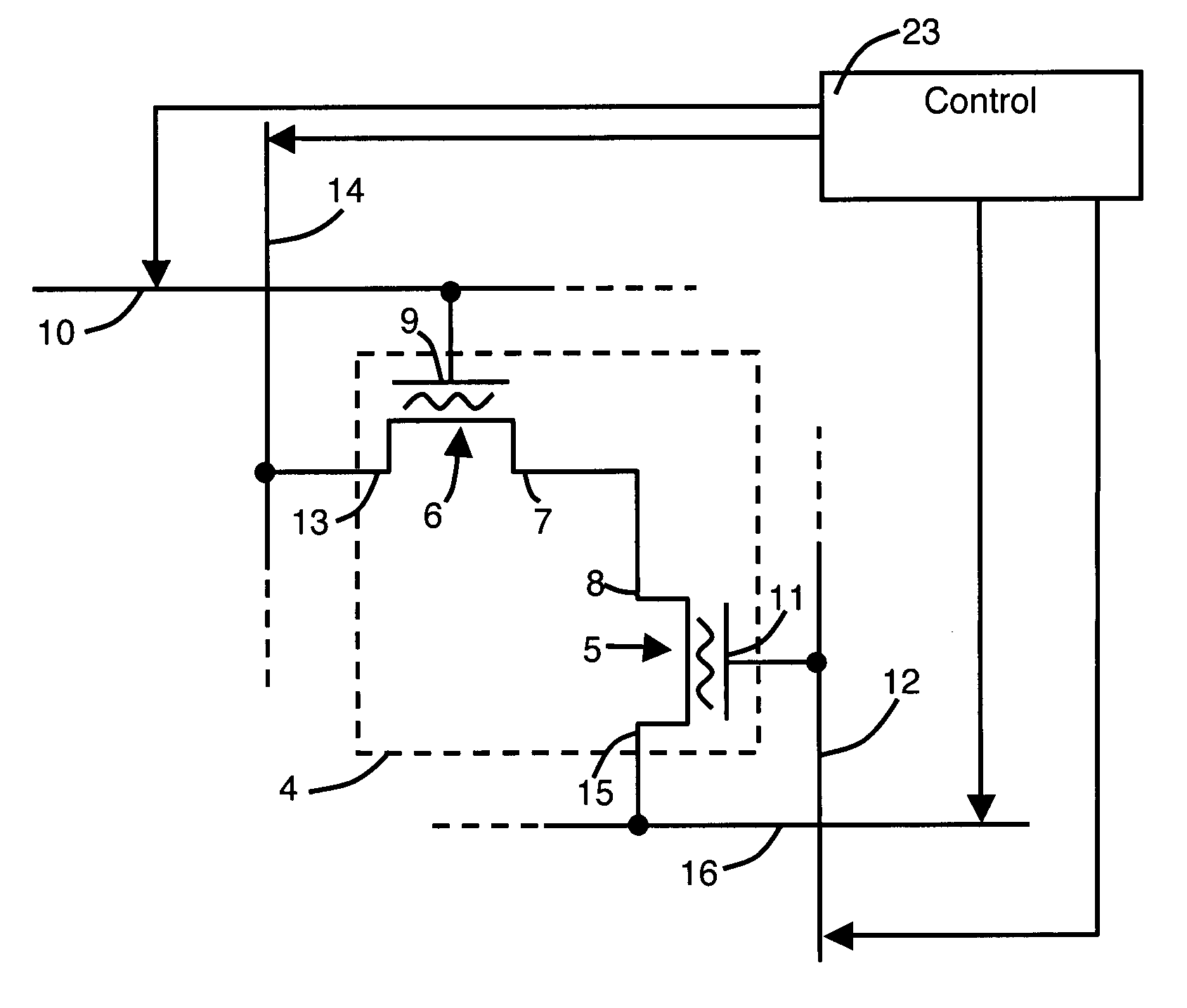
[0045]The memory cell 4 represented in FIG. 2 comprises a field effect memory transistor 5 comprising a nanowire covered by one type of memory molecules and a field effect access transistor 6 comprising a nanowire covered by said type of memory molecules. The source 7 of the access transistor 6 is connected to the drain 8 of the memory transistor 5 in such a way that the memory cell 4 forms a quadripole.

[0046]In a memory device comprising a plurality of memory cells 4, the gate 9 of the access transistor 6 is connected to a word line 10 and the gate 11 of the memory transistor 5 is connected to a write line 12. The drain 13 of the access transistor 6 is connected to a read line 14 and a source 15 of the memory transistor 5 is connected to a source line 16.

[0047]Using the same type of transistor and a single type of molecules enables the memory cell 4 to be made very compact and easy to achieve.

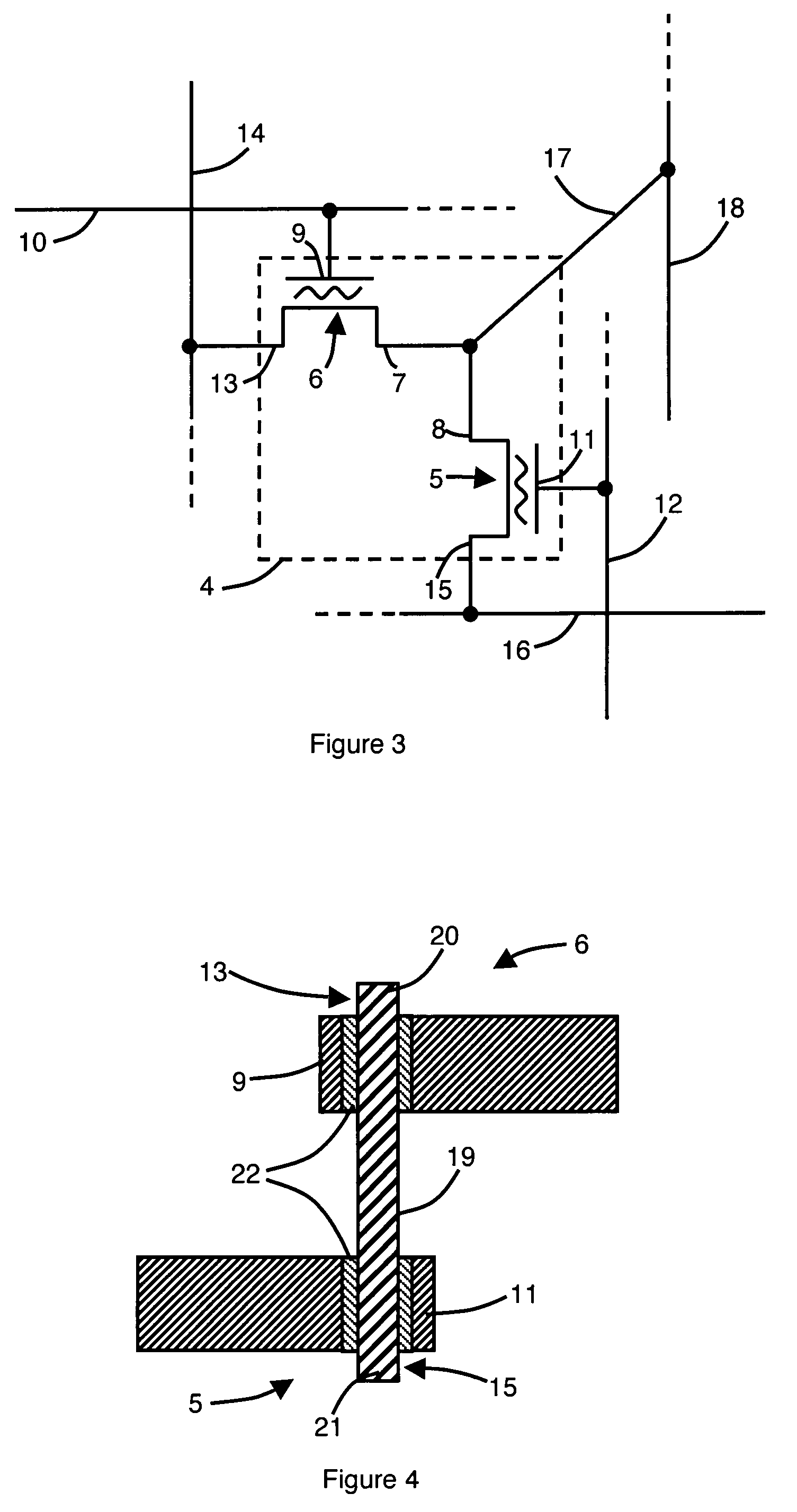
[0048]In FIG. 3, the source 7 of the access transistor 6 and the drain 8 of the memory tra...


PUM


Abstract

The memory cell comprises a field effect memory transistor comprising a nanowire covered by a type of memory molecules and an access transistor of the same type. A source of the access transistor is connected to a drain of the memory transistor. The nanowire of the access transistor and the nanowire of the memory transistor can be formed by a single nanowire having two ends respectively forming a drain of the access transistor and a source of the memory transistor. The memory device comprises a plurality of memory cells, an access transistor gate being connected to a word line and a memory transistor gate being connected to a write line.

Description

BACKGROUND OF THE INVENTION[0001]The invention relates to a memory cell comprising a field effect memory transistor comprising a nanowire covered by a type of memory molecules.STATE OF THE ART[0002]Molecular memory cells present the advantage of being fast, compact and non-volatile and can be produced in simple manner using in particular self-assembly techniques. Molecular memory cells comprise a dipolar molecular component for storing binary or multivalued data.[0003]The article “Multilevel memory based on molecular devices” by C. Li et al. (Applied Physics Letters, Vol. 84, No 11, 2004) describes a field effect memory transistor comprising a nanowire covered by memory molecules presenting several degrees of oxidation reduction representative of digital data (NWFET transistor: “Nano-wire Field Effect Transistor”). Data storing can be performed by modifying the degree of oxidation reduction, which influences the threshold voltage of the transistor. Read can be performed by measuring...

Claims


Application Information

Patent Timeline
Patent Type & Authority Patents(United States)
IPC IPC(8): G11C11/00
CPCB82Y10/00G11C13/0009G11C13/025G11C13/02G11C2213/17
Inventor JALABERT, ANTOINE
Owner COMMISSARIAT A LENERGIE ATOMIQUE ET AUX ENERGIES ALTERNATIVES
Why Eureka
Try Eureka