Thin-film piezoelectric device and method of manufacturing the same

a piezoelectric device and thin film technology, applied in the direction of device material selection, maintaining head carrier alignment, instruments, etc., can solve the problems of large warpage of substrates and cracking of ceramics, and achieve the effect of improving the reliability of the performance of the thin film piezoelectric devi

Inactive Publication Date: 2009-09-29
TOSHIBA STORAGE DEVICE CORP
View PDF16 Cites 11 Cited by
  • Summary
  • Abstract
  • Description
  • Claims
  • Application Information

AI Technical Summary

Benefits of technology

[0013]In view of the foregoing, the present invention is directed to a configuration of a thin-film piezoelectric device that prevents, even if a thin film of piezoelectric ceramic is formed on a thin substrate, cracking of the ceramic thin film and warpage of the substrate, and enhances reliability of the performance of the thin-film piezoelectric device, and a method of manufacturing the thin-film piezoelectric device.

Problems solved by technology

However, when the temperature is lowered to room temperature after ceramic crystallization by the heat treatment, the difference in thermal expansion coefficients of the ceramics and the substrates causes cracking of the ceramics and large warpage of the substrates.
This problem often occurs especially when thin substrates such as suspensions are used.

Method used


Image

  • Thin-film piezoelectric device and method of manufacturing the same
  • Thin-film piezoelectric device and method of manufacturing the same
  • Thin-film piezoelectric device and method of manufacturing the same

Examples


Embodiment Construction

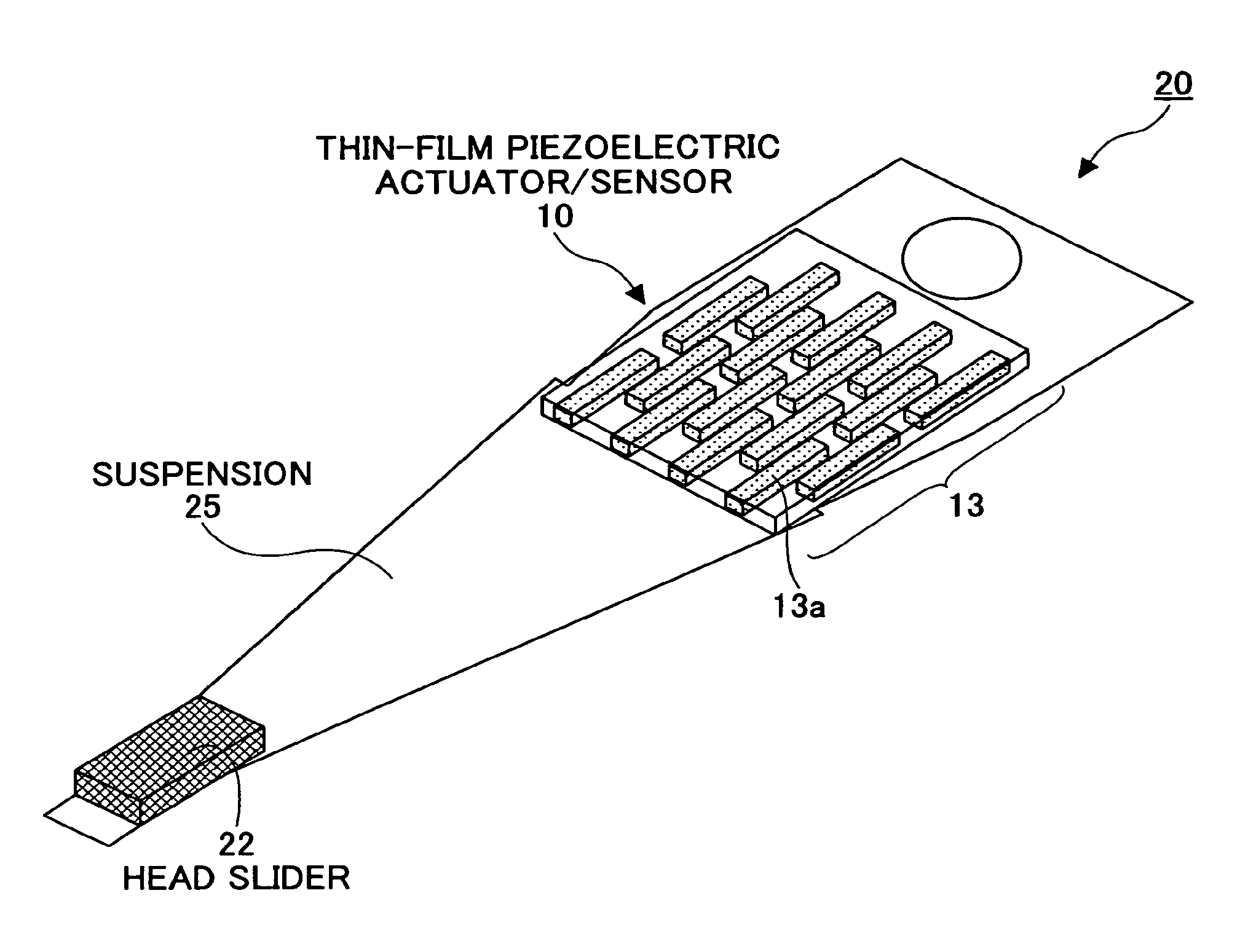
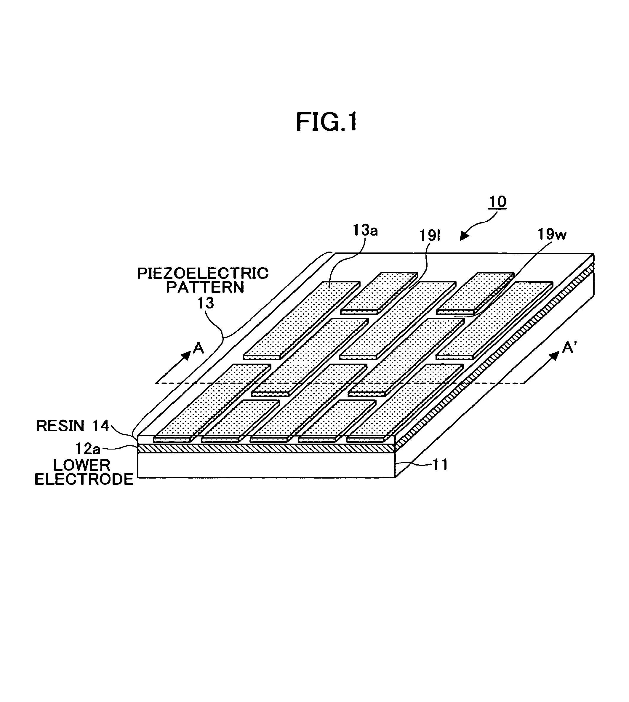
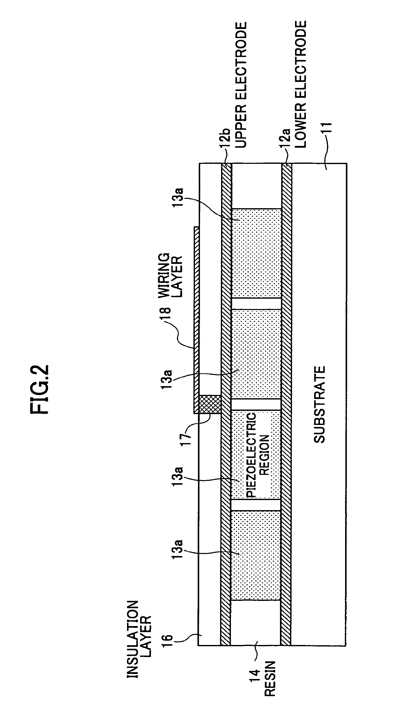
[0040]FIG. 1 is a schematic perspective view showing a part of a thin-film piezoelectric actuator / sensor 10 according to an embodiment of the present invention (an upper electrode 12b and a wiring layer 18 are not shown in order to more easily view other components). FIG. 2 is a cross-sectional view showing the thin-film piezoelectric actuator / sensor 10 taken along line A-A′ of FIG. 1.

[0041]The thin-film piezoelectric actuator / sensor 10 comprises a substrate 11, a pair of a lower electrode 12a and the upper electrode 12b disposed on the substrate 11, a piezoelectric pattern 13 disposed between the lower electrode 12a and the upper electrode 12b and including plural piezoelectric regions 13a, and resin 14 in the space between the piezoelectric regions 13a. The thin-film piezoelectric actuator / sensor 10 further comprises the wiring layer 18. The wiring layer 18 applies a voltage to the piezoelectric pattern 13 through a via contact 17, which is formed in an insulation layer 16, and th...


PUM

PropertyMeasurementUnit
temperatureaaaaaaaaaa
widthaaaaaaaaaa
thicknessaaaaaaaaaa

Abstract

A thin-film piezoelectric device is disclosed that includes a substrate, a piezoelectric pattern disposed on the substrate, the piezoelectric pattern including plural spaced-apart piezoelectric regions, and a pair of electrodes that apply an electric field to the piezoelectric pattern.

Description

BACKGROUND OF THE INVENTION[0001]1. Field of the Invention[0002]The present invention relates to a thin-film piezoelectric device and a method of manufacturing the same, and particularly relates to a thin-film piezoelectric actuator / sensor utilizing deflection of a substrate due to piezoelectric effect of ferroelectric ceramics and a method of manufacturing the same.[0003]2. Description of the Related Art[0004]Thin-film piezoelectric actuators are configured to drive objects using the piezoelectric effect of piezoelectric (electrostrictive) ceramic thin films formed on substrates. Piezoelectric substances generate a voltage in response to an applied force or stress (piezoelectric effect or electrostrictive effect). This effect is reversible. That is, piezoelectric substances are deformed in response to an applied voltage. In the following description, both the piezoelectric effect and the reversed effect are referred to as piezoelectric effect for ease of explanation.[0005]Usually, ...

Claims


Application Information

Patent Timeline
Patent Type & Authority Patents(United States)
IPC IPC(8): H01L41/08G11B21/10G11B21/21H01L41/09H01L41/18H01L41/187H01L41/22H01L41/332
CPCG11B5/58G11B5/6005H01L41/332H01L41/0805H01L41/1876H01L41/314G11B5/4873H10N30/1051H10N30/8554H10N30/074H10N30/082
Inventor AOKI, TSUYOSHIKURIHARA, KAZUAKIUMEMIYA, SHIGEYOSHI
Owner TOSHIBA STORAGE DEVICE CORP
Why Eureka
Try Eureka