Structure and manufacturing method of a chip scale package

a scale package and manufacturing method technology, applied in the direction of semiconductor devices, semiconductor/solid-state device details, electrical apparatus, etc., can solve the problems of significant degrading of chip performance, increasing negative impact on package performance, and increasing device density and device complexity, so as to improve the electrical performance of the device, shorten the interconnection, and cost-effective

Inactive Publication Date: 2008-03-20
QUALCOMM INC
View PDF99 Cites 13 Cited by
  • Summary
  • Abstract
  • Description
  • Claims
  • Application Information

AI Technical Summary

Benefits of technology

[0011] Another objective of the invention is to provide a method for shortening the interconnection between a semiconductor device and the substrate on which the device is mounted, thus improving the electrical performance of the device.
[0012] Yet another objective of the invention is to eliminate conventional methods of re-distribution of device I / O interconnect, thereby making packaging of the device more cost-effective and eliminating performance degradation.
[0013] A still further objective of the invention is to improve chip accessibility during testing of the device, thus eliminating the need for special test fixtures.
[0014] A still further objective of the invention is to improve performance and device reliability of BGA packages that are used for the mounting of semiconductor devices having small-pitch I / O interconnect bumps.

Problems solved by technology

Semiconductor device performance improvements are largely achieved by reducing device dimensions, a development that has at the same time resulted in considerable increases in device density and device complexity.
Device interconnects, due to their increase in length in order to package complex devices and connect these devices to surrounding circuitry, tend to have an increasingly negative impact on the package performance.
For longer and more robust metal interconnects, the parasitic capacitance and resistance of the metal interconnection increase, which degrades the chip performance significantly.

Method used


Image

  • Structure and manufacturing method of a chip scale package
  • Structure and manufacturing method of a chip scale package
  • Structure and manufacturing method of a chip scale package

Examples


Embodiment Construction

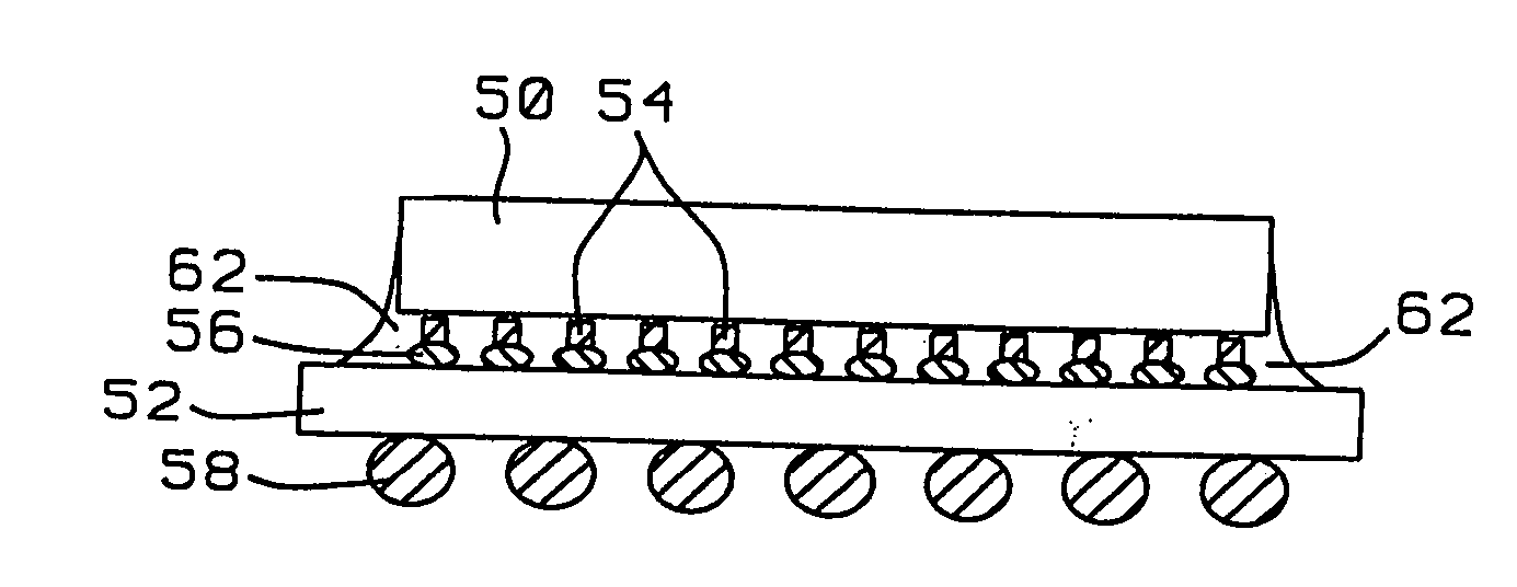
[0034] The above stated objective of improving chip accessibility during testing of the device, thus eliminating the need for special test fixtures, can further be highlighted as follows. The disclosed method of the invention, using Chip Scale Packaging (CSP), can control the cost of testing CSP devices by keeping the same body size of the chip and by using the same size substrate. For conventional CSP packages, the chip may have different body sizes, which imposes the requirement of different size test fixtures. With the continued reduction of the size of semiconductor devices, additional and varying device sizes are expected to be used. This would result in ever increasing costs for back-end testing of the devices in a production environment. The invention provides a method where these additional back-end testing costs can be avoided.

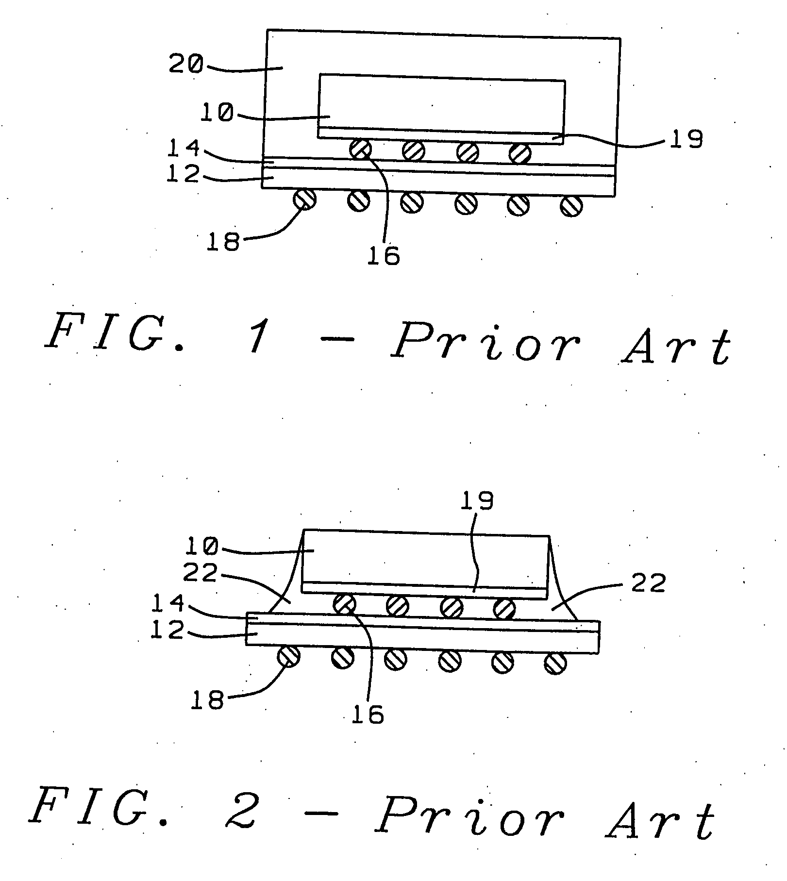
[0035] Referring now to FIG. 1, there is shown a cross section of a typical flip chip package with the semiconductor device being encapsulated in a ...


PUM


Abstract

A new method and package is provided for the mounting of semiconductor devices that have been provided with small-pitch Input/Output interconnect bumps. Fine pitch solder bumps, consisting of pillar metal and a solder bump, are applied directly to the I/O pads of the semiconductor device, the device is then flip-chip bonded to a substrate. Dummy bumps may be provided for cases where the I/O pads of the device are arranged such that additional mechanical support for the device is required.

Description

[0001] This application is a continuation of Ser. No. 09 / 837,007, filed on Apr. 18, 2001, which is a continuation-in-part of Ser. No. 09 / 798,654, filed on Mar. 5, 2001, now U.S. Pat. No. 6,818,545.BACKGROUND OF THE INVENTION [0002] (1) Field of the Invention [0003] The invention relates to the fabrication of integrated circuit devices, and more particularly, to a method and package for packaging semiconductor devices. [0004] (2) Description of the Prior Art [0005] Semiconductor device performance improvements are largely achieved by reducing device dimensions, a development that has at the same time resulted in considerable increases in device density and device complexity. These developments have resulted in placing increasing demands on the methods and techniques that are used to access the devices, also referred to as Input / Output (I / O) capabilities of the device. This has led to new methods of packaging semiconductor devices whereby structures such as Ball Grid Array (BGA) devic...

Claims


Application Information

Patent Timeline
Patent Type & Authority Applications(United States)
IPC IPC(8): H01L23/488
CPCH01L23/49816H01L24/06H01L2924/01033H01L2924/01006H01L2924/01005H01L2924/00013H01L2924/30105H01L2924/15311H01L2924/14H01L2924/12044H01L2924/04941H01L2924/014H01L24/12H01L24/16H01L24/17H01L2224/0401H01L2224/04042H01L2224/06136H01L2224/13007H01L2224/13023H01L2224/1308H01L2224/13083H01L2224/131H01L2224/13147H01L2224/13155H01L2224/16H01L2924/01002H01L2924/01013H01L2924/01014H01L2924/01015H01L2924/01018H01L2924/01022H01L2924/01029H01L2924/01042H01L2924/0105H01L2924/01073H01L2924/01074H01L2924/01075H01L2924/01078H01L2924/01079H01L2924/01082H01L2924/00014H01L2224/13099H01L2224/05572H01L2224/13017H01L2924/181H01L2924/351H01L2924/00
Inventor LIN, MOU-SHIUNGLEI, MING-TALIN, CHUEN-JYE
Owner QUALCOMM INC
Why Eureka
Try Eureka