Method for Fabricating Micro-Lens and Micro-Lens Integrated Optoelectronic Devices Using Selective Etch of Compound Semiconductor

Inactive Publication Date: 2009-03-12
GWANGJU INST OF SCI & TECH +1
View PDF8 Cites 8 Cited by
  • Summary
  • Abstract
  • Description
  • Claims
  • Application Information

AI Technical Summary

Benefits of technology

[0018]As described above, a compound semiconductor layer is formed by a digital alloy method such that the concentration of a reactive metal varies with height. Also, the compound semiconductor layer having the reactive metal, of which concentration varies with height, is partially removed to form a circular or elliptical microlens. In this process, a high-density microlens array can be fabricated. Further, since the microlens is formed of a compound semiconductor, the microlens can be monolithically grown on a substrate of the photoelectric device, and an improvement in the characteristics of the photoelectric device can be facilitated. In addition, when a photoelectric device into which a microlens is integrated is fabricated, the center of the microlens may be self-aligned with an active layer of the photoelectric device, so that the microlens can be integrated without a typical photolithography process. As a consequence, a fabrication process can be simplified, and the packaging cost of an optical communication system or optical interconnection system can be reduced.

Problems solved by technology

However, since laser beams irradiated from a surface are greatly diffused, when the VCSEL is applied to a free-space optical interconnection system, crosstalk may increase between channels, and an optical transmission distance and a tolerance in optical alignment are limited.
Also, in a chip-to-chip optical interconnection system using an optical waveguide as a light transmission medium, combination efficiency between the light source and the optical waveguide is restricted by diffusion of laser beams.
However, the above-described method makes it difficult to fabricate a high-density microlens array.
Specifically, when a distance between lenses is small, adjacent lenses are brought into contact with each other during a reflow process, so that a desired microlens array cannot be obtained.
Further, a photoelectric device 200 should be precisely aligned with the microlens 201 during a photolithography process, thus making an integration process complicated.

Method used


Image

  • Method for Fabricating Micro-Lens and Micro-Lens Integrated Optoelectronic Devices Using Selective Etch of Compound Semiconductor
  • Method for Fabricating Micro-Lens and Micro-Lens Integrated Optoelectronic Devices Using Selective Etch of Compound Semiconductor
  • Method for Fabricating Micro-Lens and Micro-Lens Integrated Optoelectronic Devices Using Selective Etch of Compound Semiconductor

Examples


Embodiment Construction

[0024]Hereinafter, exemplary embodiments of the present invention will be described in detail. However, the present invention is not limited to the exemplary embodiments disclosed below, but can be implemented in various types. Therefore, the present exemplary embodiments are provided for complete disclosure of the present invention and to fully inform the scope of the present invention to those ordinarily skilled in the art.

Exemplary Embodiment

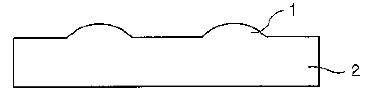
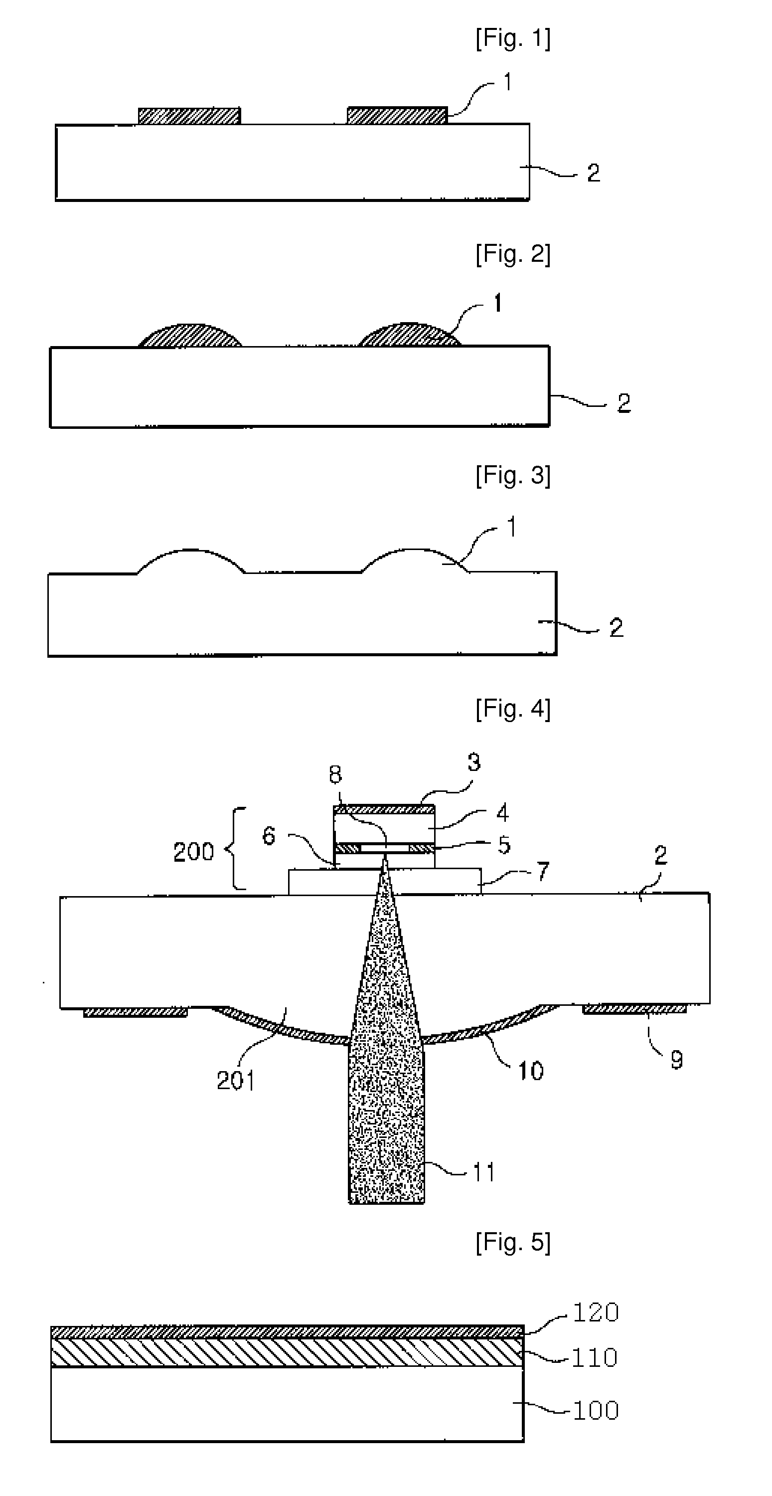
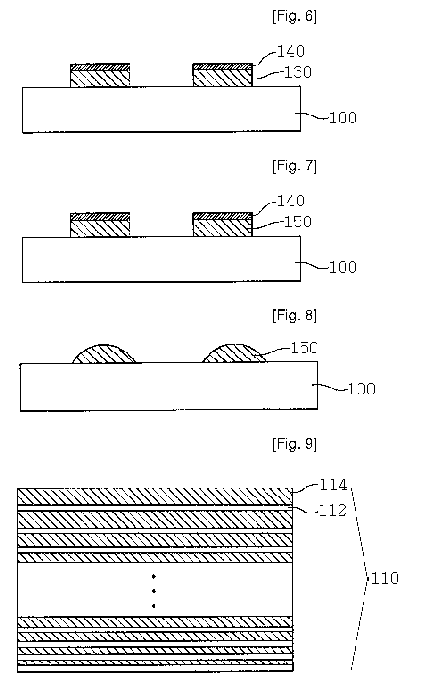
[0025]FIGS. 5 through 8 are cross-sectional views illustrating a method of fabricating a microlens using selective etching of a compound semiconductor according to an exemplary embodiment of the present invention.

[0026]Referring to FIG. 5, a compound semiconductor layer 110 is formed on a substrate 100. The compound semiconductor layer 110 contains a reactive metal. The reactive metal may be aluminum (Al). Also, the compound semiconductor layer 110 may be formed by an epitaxial growth process. The content of the reactive metal in the compound...


PUM


Abstract

Provided are a method of fabricating a microlens using selective etching of a compound semi-conductor and a method of fabricating a photoelectric device having the microlens. The formation of the microlens includes patterning a compound semiconductor layer and removing a lateral surface of the compound semiconductor layer to form a roughly hemispheric lens. The lateral surface of the compound semiconductor layer is removed by a digital alloy method. In particular, the lateral surface of the compound semiconductor layer is removed by a wet etching process.

Description

TECHNICAL FIELD[0001]The present invention relates to methods of fabricating a microlens and a photoelectric device using the microlens, and more particularly, to methods of fabricating a microlens using selective etching of a compound semiconductor and a photoelectric device having the microlens.BACKGROUND ART[0002]In recent years, the downscaling of optical systems has lead to a strong need for integration of a photoelectric device with an optical device, thus increasing the necessity and applicability of microlenses. A microlens may be integrated in a light source in order to efficiently combine optical fiber with the light source in an optical communication system, so that the entire packaging cost can be reduced. Also, since the microlens may be integrated in an optical detector to condense light into an active layer of the optical detector, the efficiency of the optical detector may be enhanced. Further, the microlens may be formed over a color filter of an image sensor to ele...

Claims


Application Information

Patent Timeline
IPC IPC(8): H01L21/00G02B3/08
CPCG02B3/0012G02B3/00
Inventor CHANG, KI-SOOLEE, YONG-TAKKAMAL, ALAMEH
Owner GWANGJU INST OF SCI & TECH
Why Eureka
Try Eureka