Differential input circuit with process variation and temperature compensation

a differential input circuit and temperature compensation technology, applied in the field of radio frequency signal processing circuitry, can solve the problems of billion dollar inventory visibility problem, inability to meet the needs of customers, so as to increase the sensitivity of the receiving a

Inactive Publication Date: 2009-11-03
ZEST LABS INC
View PDF17 Cites 5 Cited by
  • Summary
  • Abstract
  • Description
  • Claims
  • Application Information

AI Technical Summary

Problems solved by technology

However, the bar code still requires manual interrogation by a human operator to scan each tagged object individually with a scanner.
This is a line-of-sight process that has inherent limitations in speed and reliability.
In transit, these outer labels are often damaged or lost.
Error rates at each point in the supply chain have been 4-18% thus creating a billion dollar inventory visibility problem.
Early field trials have shown that the currently available passive short-range Class-1 and Class-2 tags are often inadequate for tagging pallets and many types of cases.
The problems with these passive tags are particularly severe when working with “RF-unfriendly” materials like metal (like soup cans), metal foils (like potato chips), or conductive liquids (like soft drinks, shampoo).
It is very difficult if not impossible to consistently read case tags located in the interior of a stack of cases, as occurs in a warehouse or pallet.
The existing passive tags are also inadequate to tag large or rapidly moving objects like trucks, cars, shipping containers, etc.
Thus, AM-Detector circuits implementing traditional diodes or transistors are not sensitive enough for long range use.
However, both zero-bias Schottky diodes and zero-threshold MOS devices are sensitive to temperature, and are affected by process variations.
More particularly, even with these feature-added devices, the conventional RF AM-Detector circuits suffer from the receiving sensitivity loss caused by ambient temperature changes and the foundry's inherent process variations.
The forward bias voltage of a Schottky diode or the threshold voltage of a MOS device could potentially vary by more than 200 mV over a 100° C. temperature range, a large issue where the device is attempting to detect millivolt signals.
This problem is an ongoing concern, as many commercial products are used in temperatures ranging, for example, from −5° C. to 70° C. in outdoor and refrigerated or heated environments; while industrial and military products cover even wider temperature ranges such as −40° C. to 85° C. and −55° C. to 125° C., respectively, in applications from cold storage to heated processing environments to high altitude and outer space applications.

Method used


Image

  • Differential input circuit with process variation and temperature compensation
  • Differential input circuit with process variation and temperature compensation
  • Differential input circuit with process variation and temperature compensation

Examples


Embodiment Construction

[0046]The following description is the best embodiment presently contemplated for carrying out the present invention. This description is made for the purpose of illustrating the general principles of the present invention and is not meant to limit the inventive concepts claimed herein.

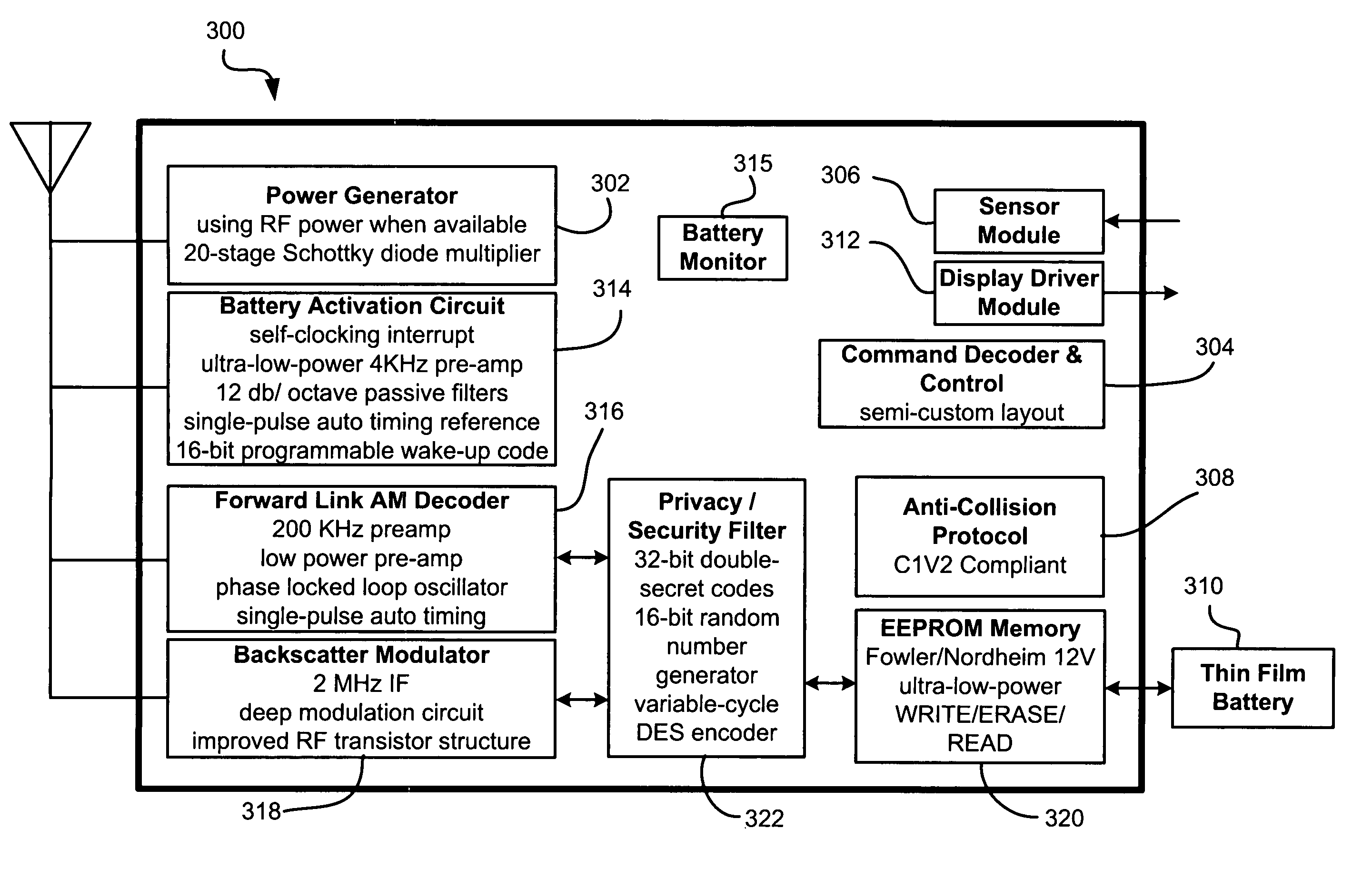
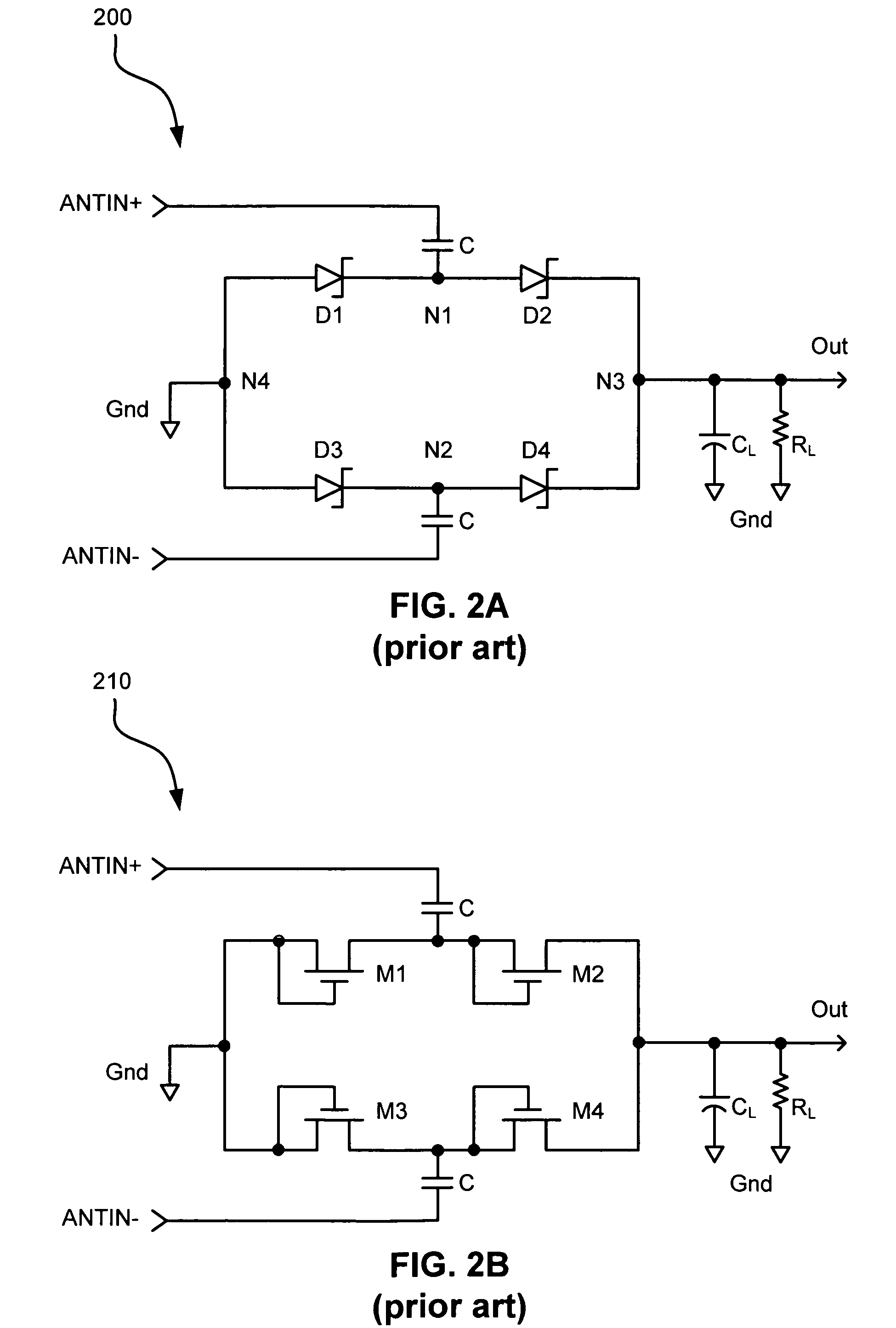
[0047]The following specification describes systems capable of using normal threshold N-Channel MOS (NMOS) and other types of semiconductor devices which are DC-biased at their inversion region. The “inversion region” collectively refers to a point in the weak inversion (i.e., sub-threshold) region and the strong inversion region (at threshold and above) of the semiconductor device. In an AM detection application, these either weakly or strongly turned-on semiconductor devices will increase the receiving AC sensitivity of an AM-Detector as compared to that of a conventional AM-Detector (FIGS. 2A-C) using normal threshold NMOS devices without any DC-biasing. The disclosed circuits are also useful in ch...


PUM


Abstract

Systems with semiconductor devices that are DC-biased at either their weak inversion (i.e., sub-threshold) region or their strong inversion region. In a preferred embodiment using semiconductor devices (e.g., NMOS, PMOS, etc.), a gate to source voltage (Vgs) is slightly below the threshold voltage (Vtn) of the device. These weakly turned-on semiconductor devices increase the receiving AC sensitivity of an AM-Detector compared to that of a conventional AM-Detector without any DC-biasing. Further, the compensating bias voltage (Vbias) compensates for one or both of the ambient temperature change and the foundry's process variation of the various semiconductor devices.

Description

FIELD OF THE INVENTION[0001]The present invention relates to Radio Frequency (RF) signal processing circuitry, and more particularly, this invention relates to biased signal processing circuitry for RF tags and other RF devices.BACKGROUND OF THE INVENTION[0002]Automatic identification (“Auto-ID”) technology is used to help machines identify objects and capture data automatically. One of the earliest Auto-ID technologies was the bar code, which uses an alternating series of thin and wide bands that can be digitally interpreted by an optical scanner. This technology gained widespread adoption and near-universal acceptance with the designation of the universal product code (“UPC”)—a standard governed by an industry-wide consortium called the Uniform Code Council. Formally adopted in 1973, the UPC is one of the most ubiquitous symbols present on virtually all manufactured goods today and has allowed for enormous efficiency in the tracking of goods through the manufacturing, supply, and ...

Claims


Application Information

Patent Timeline
Patent Type & Authority Patents(United States)
IPC IPC(8): G06K19/06G08B13/14
CPCH03D1/10
Inventor SHYU, JYN-BANG
Owner ZEST LABS INC
Why Eureka
Try Eureka