Active matrix substrate and display device including the same

a technology of active matrix substrate and substrate, which is applied in the direction of semiconductor devices, instruments, optics, etc., can solve the problems of reducing display quality, reducing display quality, and inconsistency in relative positions (positional relationships) between patterns, so as to reduce block segmentation and flickering, avoid decreased aperture ratio, and increase parasitic capacity and complication

Inactive Publication Date: 2009-11-03
SHARP KK
View PDF22 Cites 12 Cited by
  • Summary
  • Abstract
  • Description
  • Claims
  • Application Information

AI Technical Summary

Benefits of technology

[0028]In order to overcome the problems described above, preferred embodiments of the present invention provide an active matrix substrate capable of decreasing block segmentation and flickering due to separate exposure while avoiding decreased aperture ratio, increased parasitic capacity and complication in the manufacturing process, and provide a display device including such an active matrix substrate.

Problems solved by technology

Generally, the exposure step, performed by using exposure equipment such as a stepper, involves various error factors in terms of stage positioning accuracy, focus level, etc., and these factors cause inconsistency in relative positions (positional relationships) between the patterns (layers).
This phenomenon, which is sometimes called “block segmentation” (or “tiling”), decreases display quality.
Therefore, differences in the level shift ΔVd among the segmented regions will unavoidably result in a situation that the asymmetry correction is imperfect in some of the regions, leading to a problem of flickering (of the display) which decreases display quality.
However, active matrix substrates such as those disclosed in Patent Documents 1 through 3 have a problem.
This also increases the level shift ΔVd (absolute value) (of the pixel electric potential) given by the mathematical expression (1), making it difficult to correct the level shift ΔVd by an electric potential Vcom applied to the opposed electrode Ec, resulting in such problems as deterioration of the liquid crystal caused by a direct current component applied to the liquid crystal layer, decreased display quality caused by flickering, etc.
Another problem caused by increased parasitic capacity Cgd is increased delay in signal propagation, such as in scanning signals in the scanning signal lines and data signals in the data signal lines.
These delays also decrease quality of display.
Further, increased parasitic capacity per pixel leads to increased power consumption in the drive circuit of the active matrix substrate.
Further, formation of a TFT for each subpixel and formation of a new capacity for each pixel require complicated mask patterns in the manufacture of the active matrix substrate, and can decrease production yield of the active matrix substrate.
However, the decrease in parasitic capacity inconsistency achievable by such an improvement alone is not sufficiently more significant than the levels achieved by the other conventional techniques described above, and so it is not possible to provide a satisfactory solution to the problems of block segmentation and annoying levels of flickering.

Method used


Image

  • Active matrix substrate and display device including the same
  • Active matrix substrate and display device including the same
  • Active matrix substrate and display device including the same

Examples


second preferred embodiment

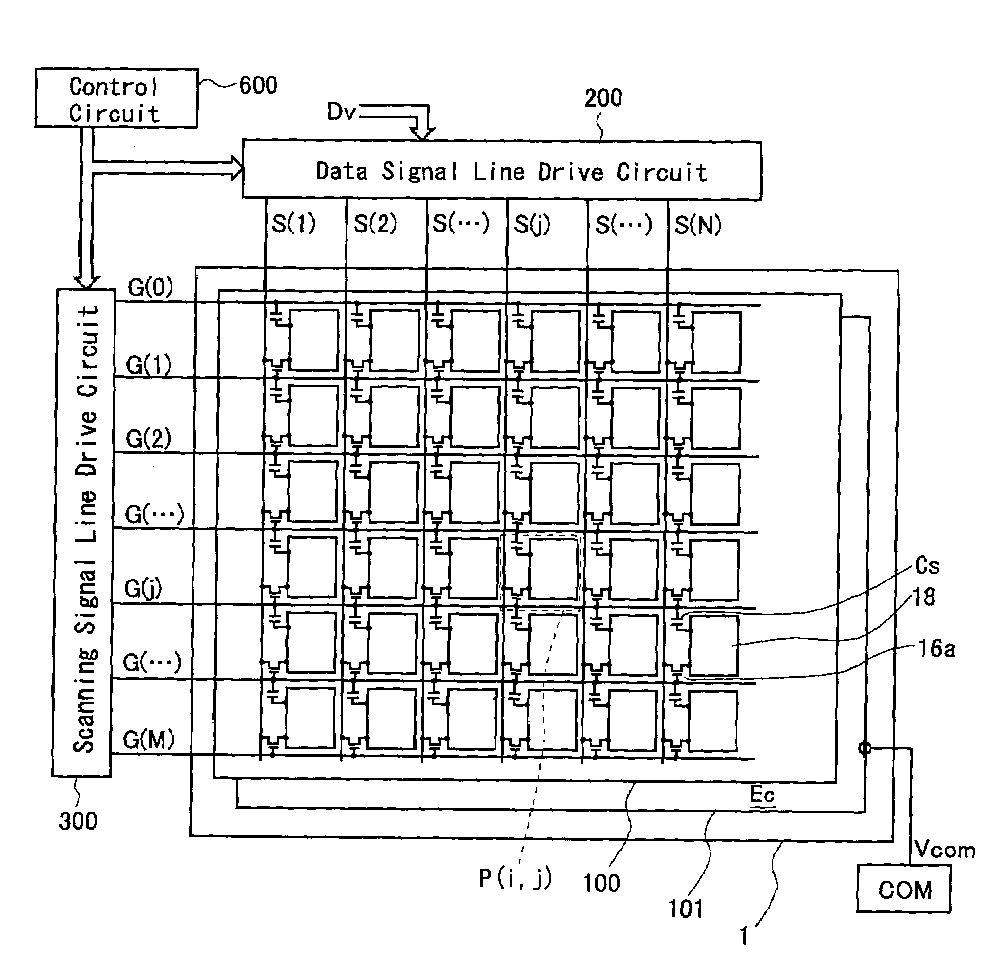
[0128]FIG. 8 is a block diagram which shows an overall configuration of a liquid crystal display device including a TFT substrate which is an active matrix substrate according to a second preferred embodiment of the present invention. Differing from the first preferred embodiment, the liquid crystal display device includes: a plurality of auxiliary capacity lines CS (1) through CS (M) extending in parallel to respective scanning signal lines G(1) through G(M) formed on the TFT substrate 100b; and two auxiliary capacity line drive circuits CS for supplying a common electrode potential Vcs to each of the auxiliary capacity lines CS(1) through CS (M) from their first and second ends. All the other aspects of the configuration than these are identical with those of the liquid crystal display device (FIG. 1) which uses the TFT substrate 100 according to the first preferred embodiment; therefore, those identical or corresponding elements are indicated by the same reference symbols, and th...


PUM

PropertyMeasurementUnit
electrostatic capacitanceaaaaaaaaaa
dispersionaaaaaaaaaa
areaaaaaaaaaaa

Abstract

It is possible to decrease block segmentation and flickering due to separate exposure in an active matrix substrate while avoiding decreased aperture ratio, increased parasitic capacity and complication in manufacturing process. A first pixel circuit and a second pixel circuit including a first-type TFT and a second-type TFT, respectively, are disposed alternately relative to each other in both directions of row and column in an active matrix substrate. In the first-type and the second-type TFTs, a pattern misalignment of the drain electrode with respect to the gate electrode in an up-down direction will increase / decrease a gate-drain parasitic capacity Cgd in reverse ways. By disposing these two types of TFTs in uniform dispersion, the increase / decrease in the parasitic capacity Cgd caused by pattern misalignment occurring at the time of manufacture are averaged.

Description

BACKGROUND OF THE INVENTION[0001]1. Field of the Invention[0002]The present invention relates to active matrix substrates used in matrix type liquid crystal display devices, EL (electroluminescence) display devices, etc. More specifically, the present invention relates to an active matrix substrate which includes: a plurality of data signal lines and a plurality of scanning signal lines disposed in a grid pattern that provide intersections; and a matrix of pixel circuits each corresponding to one of the intersections and having a switching element provided by, e.g., a field-effect transistor such as a thin-film transistor, and a voltage holding capacitor; and relates also to a display device which includes the active matrix substrate.[0003]2. Description of the Related Art[0004]Active matrix substrates are utilized widely in active matrix type display devices such as liquid crystal display devices and EL display devices, as well as active matrix type sensors. In particular, liquid c...

Claims


Application Information

Patent Timeline
Patent Type & Authority Patents(United States)
IPC IPC(8): G02F1/136
CPCG02F1/1362H01L27/124G09G3/3648H01L27/3262H01L29/41733H01L29/42384H01L27/1255G02F1/1368G02F2001/13606G09G3/3233G09G3/3614G09G2300/0443G09G2300/0842G09G2300/0847G09G2310/0262G09G2320/0209G09G2320/0233H01L27/3211H01L27/3276G02F1/13606H10K59/35H10K59/1213H10K59/131
Inventor HISADA, YUHKO
Owner SHARP KK
Why Eureka
Try Eureka