Method for producing multijunction solar cell

a solar cell and multi-junction technology, applied in the direction of basic electric elements, electrical apparatus, semiconductor devices, etc., can solve the problems of reducing crystal quality, and achieve the effect of increasing the area of the devi

Inactive Publication Date: 2009-11-10
HONDA MOTOR CO LTD
View PDF2 Cites 16 Cited by
  • Summary
  • Abstract
  • Description
  • Claims
  • Application Information

AI Technical Summary

Benefits of technology

[0014]An object of the present invention is to provide a method for producing a multijunction solar cell which can eliminate such a disadvantage to achieve a multijunction solar cell having four junctions and increase the area of a device.
[0018]Therefore, in the first aspect of the production method of the present invention, the second semiconductor having a narrower band gap than the first semiconductor is grown on the first semiconductor. In this way, the second semiconductor can be grown in the shape of a wire without reducing the crystal quality of the first semiconductor that is already grown in the shape of a wire.
[0019]As a result, according to the production method of the present invention, the second wire-shaped semiconductor can be grown epitaxially on the first wire-shaped semiconductor, thereby capable of forming the first single-junction solar cell comprising the second semiconductor. Moreover, at this time, it is possible to provide excellent performance to the first single-junction solar cell by preventing the occurrence of dislocation in the second semiconductor by interposing the first semiconductor comprising the same material as the substrate between the substrate and the first single-junction solar cell.
[0026]In the second aspect of the production method of the present invention, the second semiconductor having a narrower band gap than the first semiconductor is grown on the first semiconductor. Therefore, the second semiconductor can be grown in the shape of a wire without reducing the crystal quality of the first semiconductor that is already grown in the shape of a wire. As a result, the second wire-shaped semiconductor can be grown epitaxially on the first wire-shaped semiconductor, thereby capable of forming the multijunction solar cell comprising the first single-junction solar cell comprising the first semiconductor and the second single-junction solar cell comprising the second semiconductor.
[0031]When forming a multijunction solar cell with four junctions in the manner as described in the aspects of the production method of the present invention, a multijunction structure in which each junction involves different semiconductors will be formed by wire-shaped semiconductors. As a result, a junction interface of the wire-shaped semiconductors has a very small area, which relieves the distortion resulting from the difference of the lattice constants and can prevent the occurrence of defects. Therefore, the limit of selecting materials resulting from the difference of the lattice constants can be mitigated to increase the alternatives for combining materials.

Problems solved by technology

However, if such a procedure is employed, the semiconductor having a narrower band gap already grown in the shape of a wire will be deteriorated to reduce the crystal quality while the semiconductor having a wider band gap is growing in the shape of a wire.

Method used


Image

  • Method for producing multijunction solar cell
  • Method for producing multijunction solar cell
  • Method for producing multijunction solar cell

Examples


Embodiment Construction

[0039]Next, the embodiments of the present invention will be described in more detail with reference to the attached drawings.

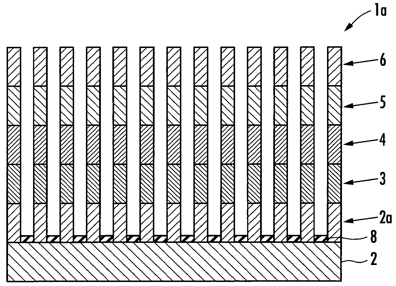
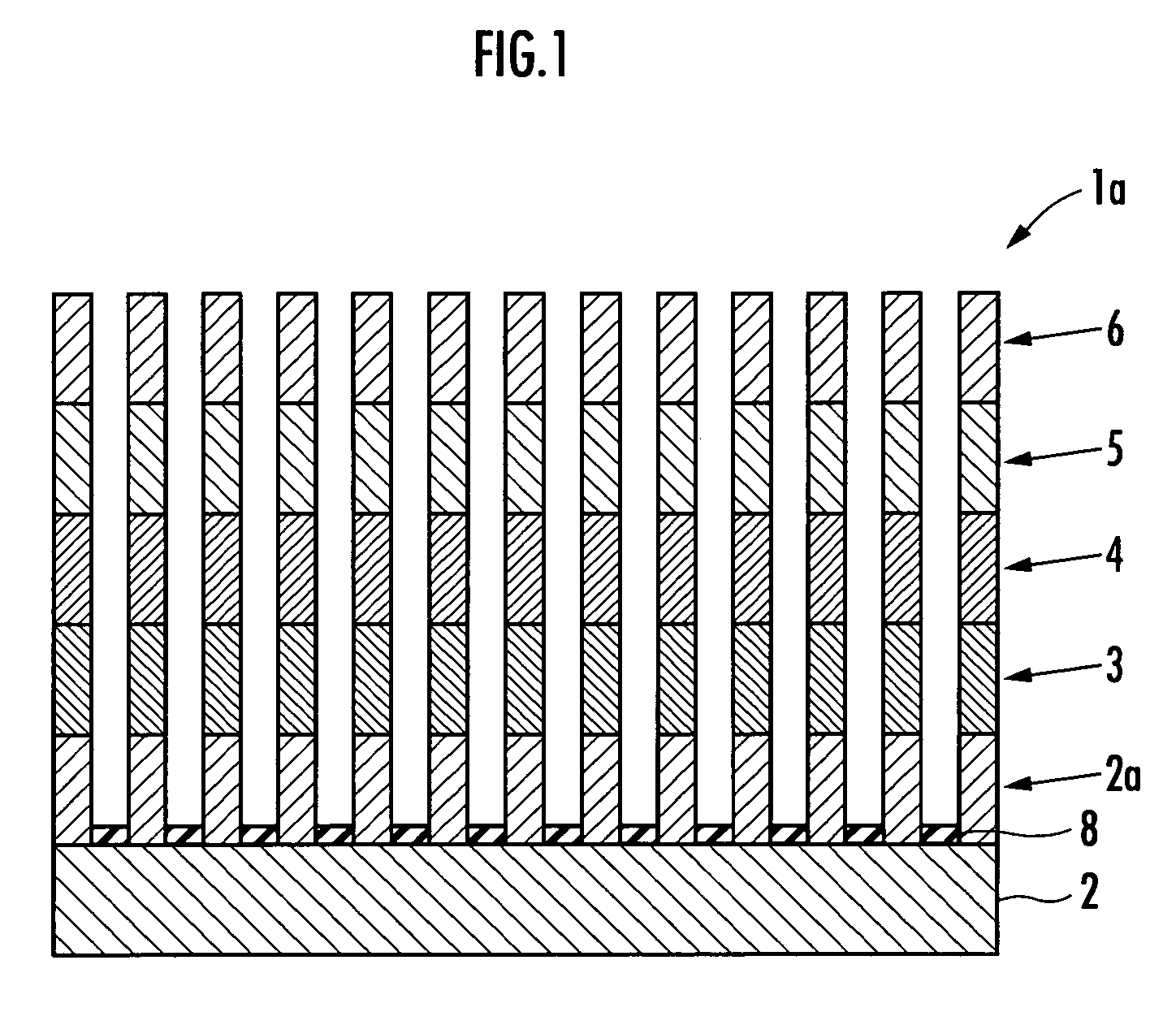
[0040]As shown in FIG. 1, a multifunction solar cell 1a obtained by the production method of the present embodiment comprises a substrate 2, a first semiconductor 2a grown in the shape of a wire on the substrate 2, a second semiconductor 3 which is connected to an end located farther from the substrate 2 of the first semiconductor 2a and is grown in the shape of a wire, a third semiconductor 4 which is connected to an end located farther from the substrate 2 of the second semiconductor 3 and is grown in the shape of a wire, a fourth semiconductor 5 which is connected to an end located farther from the substrate 2 of the third semiconductor 4 and is grown in the shape of a wire, and a fifth semiconductor 6 which is connected to an end located farther from the substrate 2 of the fourth semiconductor 5 and is grown in the shape of a wire. In the multijunction so...


PUM


Abstract

There is provided a method for producing a multijunction solar cell having four-junctions, the method allowing the area of a device to be increased. On a nucleation site formed on a substrate 2, is grown a semiconductor 2a comprising the same material as the substrate 2 in the shape of a wire. On the semiconductor 2a, are successively grown semiconductors 3, 4, 5, and 6 with a narrower band gap in the shape of a wire. The semiconductor 3 may be directly grown in the shape of a wire on the nucleation site formed on the substrate 2. It is preferred to form the nucleation site by forming an amorphous SiO2 coating 8a on the substrate 2 and etching a part of the amorphous SiO2 coating 8a. Further, it is preferred to form an insulating film 8 in the region except the nucleation sites on the substrate 2 by allowing the amorphous SiO2 coating 8a to remain therein. The semiconductor 2a is GaP; the semiconductor 3 is Al0.3Ga0.7As; the semiconductor 4 is GaAs; the semiconductor 5 is In0.3Ga0.7As; and the semiconductor 6 is In0.6Ga0.4As.

Description

BACKGROUND OF THE INVENTION[0001]1. Field of the Invention[0002]The present invention relates to a method for producing a multijunction solar cell.[0003]2. Description of the Related Art[0004]Conventionally, a single-junction solar cell comprising a single pn junction has been known. However, it is known that the power generation efficiency of the single-junction solar cell is only about 30% under terrestrial sunlight irradiation conditions irrespective of kind of semiconductor materials used, because the power generation efficiency has a theoretical limit determined by the band gap Eg of a semiconductor material used as a raw material.[0005]Thus, in order to obtain power generation efficiency higher than that of the single-junction solar cell, there is proposed a multijunction solar cell formed by laminating a plurality of solar cells in which each cell has a pn junction. As the simplest of the multijunction solar cells, there is known a two-junction solar cell 11 as shown in FIG. ...

Claims


Application Information

Patent Timeline
Patent Type & Authority Patents(United States)
IPC IPC(8): H01L21/00
CPCH01L31/035281H01L31/03529H01L31/1844H01L31/0687Y02E10/544
Inventor GOTO, HAJIMEMOTOHISA, JUNICHIFUKUI, TAKASHI
Owner HONDA MOTOR CO LTD
Why Eureka
Try Eureka