Surface inspection method and surface inspection apparatus

a surface inspection and surface technology, applied in the field of surface inspection methods and surface inspection apparatus, can solve problems such as the difficulty of detecting defects in the region concerned, and achieve the effect of preventing the influence of a noise componen

Active Publication Date: 2009-11-10
HITACHI HIGH-TECH CORP
View PDF19 Cites 9 Cited by
  • Summary
  • Abstract
  • Description
  • Claims
  • Application Information

AI Technical Summary

Benefits of technology

[0004]An object of the present invention is to provide an inspection method and inspection apparatus for preventing the influence of a noise component that generates from an object to be inspected when inspecting the surface of the object to be inspected with a beam.
[0009]According to yet another aspect of the present invention, in order to vary the amount of the received light, the light is received so that the diffracted light from the edge region of the object to be inspected may decrease.
[0016]According to the present invention, it is possible to provide an inspection method and inspection apparatus that prevent the influence of a noise component when inspecting the surface of an object to be inspected via a beam, the noise component generating from the object to be inspected.

Problems solved by technology

In the conventional art described above, due to the influence of diffracted light from a specified region (for example, edge region) of an object to be inspected, a noise component increases and a signal from the foreign matter is buried, so that it is difficult to detect defects of the region concerned.

Method used


Image

  • Surface inspection method and surface inspection apparatus
  • Surface inspection method and surface inspection apparatus
  • Surface inspection method and surface inspection apparatus

Examples


Embodiment Construction

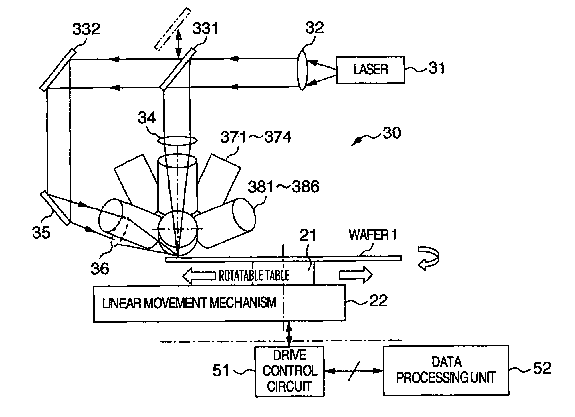
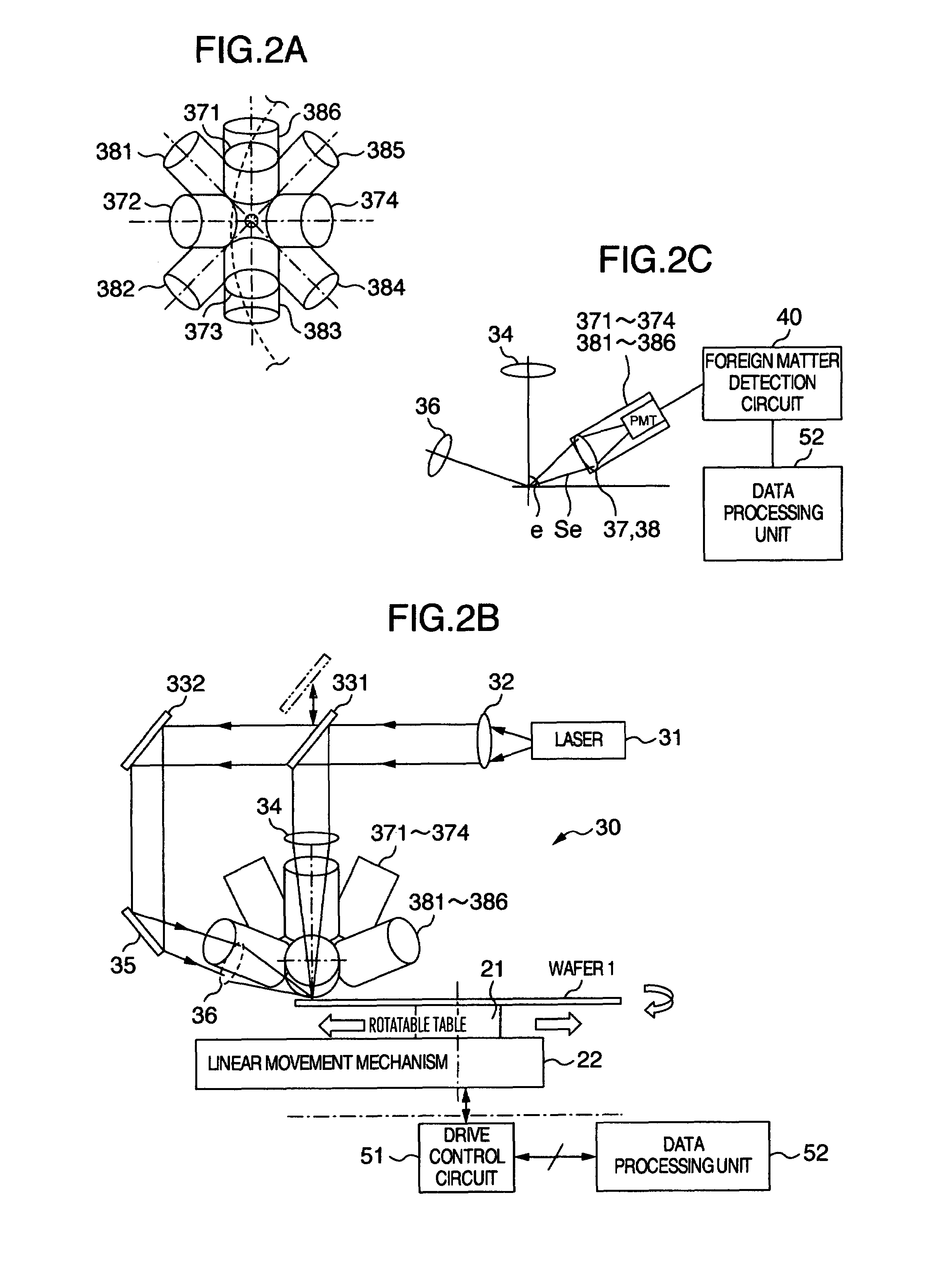
[0021]The surface inspection method and surface inspection apparatus of the present invention can be applicable to the objects to be inspected, such as a semiconductor wafer, a wafer-shaped object, an insulator wafers (e.g., a sapphire glass wafer, a silica glass wafer, and the like). As an example, an embodiment applied to the surface inspection of a semiconductor wafer is described next.

[0022]A silicon wafer serving as the base material for semiconductor ICs is manufactured from a highly purified polycrystalline silicon. The silicon wafer is manufactured by preparing a single-crystal silicon ingot via a CZ method, and slicing this into thin plates, and polishing the surface and outer peripheral edge of the sliced thin plate to a mirror surface, and then washing foreign matters sticking to the surface thereof.

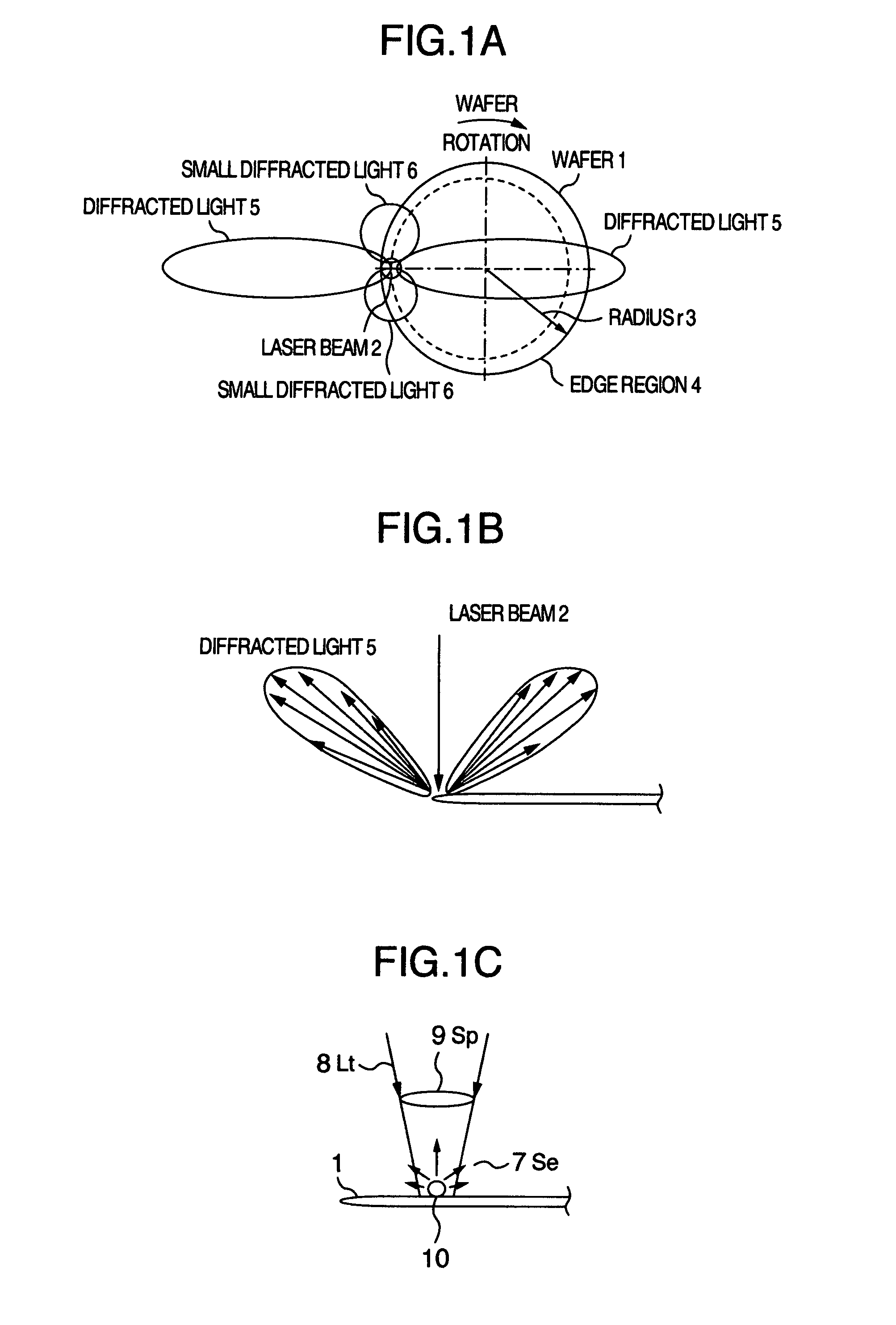
[0023]During these manufacture processes, a foreign matter or a crack may occur in the outer peripheral edge of a wafer. Defects, such as a foreign matter and a scratch in the...


PUM

PropertyMeasurementUnit
elevation angleaaaaaaaaaa
angleaaaaaaaaaa

Abstract

When measuring an edge region, a photo detector with an angle not influenced by the diffracted light, the diffracted light causing noise, is selected to thereby allow for inspection that minimizes the sensitivity reduction. This allows for the management of foreign matters in the outer peripheral portion, which conventionally could not be measured, and this also eliminates the oversight of critical defects on the wafer, thus leading to reduction of failures of IC.

Description

BACKGROUND OF THE INVENTION[0001]The present invention relates to a surface inspection method and surface inspection apparatus of an object to be inspected.[0002]Examples of the surface inspection method and surface inspection apparatus of an object to be inspected include a method and apparatus for inspecting the surface of a wafer as described in JP-A-9-304289, for example. A laser beam outputted from a laser beam source is focused into a laser spot Sp (hereinafter, referred to as a spot Sp) by a lens system and is projected approximately perpendicularly or obliquely onto the surface of a wafer, and the surface of a wafer is spirally scanned corresponding to a displacement of the wafer, and as a result the whole surface of the wafer is scanned. When a foreign matter e is present on the surface of a wafer, a scattered light Se is generated in a wide range of angles (directions). A part thereof is condensed with a condenser lens and is received by a plurality of photomultiplier tube...

Claims


Application Information

Patent Timeline
Patent Type & Authority Patents(United States)
IPC IPC(8): G01N21/00
CPCG01N21/9503G01N21/94
Inventor OKAWA, TAKASHIMITOMO, KENJI
Owner HITACHI HIGH-TECH CORP
Why Eureka
Try Eureka