Switched impedance transformer for semiconductor circuits

a transformer and impedance technology, applied in the direction of transmission, inductance, amplifier, etc., can solve the problems of increasing the difficulty of provisioning not only in the context, the cost of electrical consumption in the infrastructure of the network, and the importance of power

Active Publication Date: 2009-11-10
SIGE SEMICON EURO
View PDF8 Cites 24 Cited by
  • Summary
  • Abstract
  • Description
  • Claims
  • Application Information

AI Technical Summary

Problems solved by technology

For the system operator, power is an important aspect of cost.
The microwave infrastructure costs of the network include the cost of electrical consumption.
Therefore, as more power is required, the more costly and the more difficult it is to provision not only in the context of a remote site, but also in today's urban environments where cellular density is increasing with microcells and picocells.
A poor match often results in the transmission device purposefully increasing the output power of the amplifier to compensate for the lost power, thereby increasing overall power consumption.
This results in a significant voltage across the output transistor devices when a significant current flows, and hence significant power dissipation.
For the case of reducing the output power of an amplifier increasing the load impedance presented to the amplifier results in an increase of the output voltage swing, resulting in a smaller signal across the output transistor devices and therefore reduced power dissipation and increased efficiency.

Method used


Image

  • Switched impedance transformer for semiconductor circuits
  • Switched impedance transformer for semiconductor circuits
  • Switched impedance transformer for semiconductor circuits

Examples


first embodiment

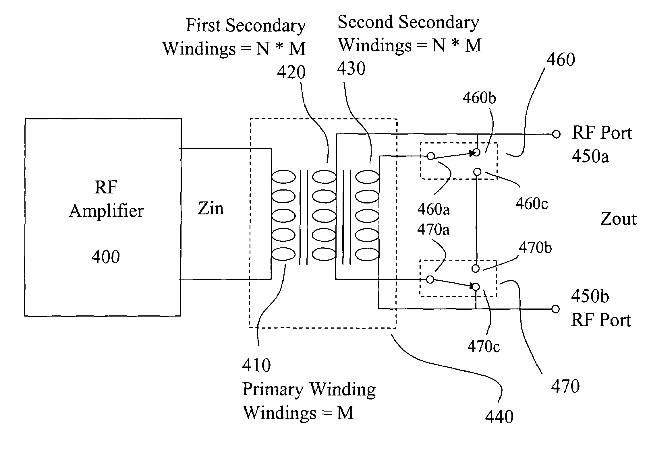
[0035]FIG. 4A illustrates the invention wherein the microwave impedance transformer is configured to a first state providing a 4:1 impedance transform. In this embodiment, a transformer 440 is disposed between an RF amplifier 400 and its RF output ports 450a and 450b.

[0036]As shown, the transformer 440 comprises three windings, a primary winding 410 comprising M turns, a first secondary winding 420 comprising N*M turns, and a second secondary winding 430 also comprising N*M turns. The primary winding 410 is connected across the output ports of the RF amplifier 400.

[0037]The first secondary winding 420 has one port electrically coupled to both the RF output port 450a and switch contact 460b of a first switching circuit 460. The other port of the first secondary winding 420 is electrically coupled to pole switch contact 470a of a second switching circuit 470.

[0038]The second secondary winding 430 has one port electrically coupled to both the RF output port 450b and switch contact 470...

second embodiment

[0043]FIG. 5 illustrates the invention wherein a microwave transformer provides one of eight impedance transforms. At high frequencies, such as encountered in RF and microwave circuits, the windings of the transformer are best considered as a series of transmission lines rather than lumped elements. As such a low frequency equivalent circuit for these devices is such that the transmission line winding is represented by an inductance, and when combining multiple windings phase effects should be considered. In this manner, a transformer operating at microwave and RF frequencies operates differently to its low frequency equivalent, for example for applications such as power transmission.

[0044]Shown in FIG. 5 is an RF input port 500, which is electrically coupled to the common contact 501a of the first switch circuit 501. The upper output port 501b of the first switch circuit 501 is electrically coupled to a first input port 510a of the transformer 510, and the lower output port 501c of...


PUM


Abstract

A method of providing an impedance match for an integrated semiconductor circuit to other microwave elements is provided by allowing the selection of one of a plurality of impedance matching ratios between the circuit and other elements. The tunable impedance match comprises a microwave impedance transformer with at least a single primary winding, and a plurality of secondary windings, wherein the winding configuration is determined by an electrical switching apparatus allowing the secondary windings to be connected in series, parallel and combinations thereof to provide the required impedance matching. The method allows for both dynamic matching of an integrated semiconductor circuit for increased efficiency, and hence reduced power consumption, and directly matching said circuit to high impedance antennae etc.

Description

FIELD OF THE INVENTION[0001]The invention relates to the field of impedance matching semiconductor circuits to external antenna, and more specifically the dynamic matching for reduced power consumption in mobile devices.BACKGROUND OF THE INVENTION[0002]In the past sixty years, the use of wireless and RF technology has increased dramatically, and in ways few could have foreseen, from limited military radar applications to today's ubiquitous penetration of wireless and microwave technology. The applications have expanded immensely but equally also have the volumes and customer base as applications such as RFID and cellular telephony have taken hold, but also in terms of functionality and complexity, and expectations of the consumers and users of these systems.[0003]Today the plain old telephone for most people is now a portable, highly compact and light communications centre which provides not only telephony but also Internet access for email, web browsing and up-loading or downloadin...

Claims


Application Information

Patent Timeline
Patent Type & Authority Patents(United States)
IPC IPC(8): H04B1/06
CPCH03F1/02H03F1/565H03F3/195H03H7/40H03F3/211H01F30/04H01F2017/0046H03F2200/318H03F2200/451H03F2200/534H03F2200/537H03F2200/541
Inventor MACPHAIL, PHILIP
Owner SIGE SEMICON EURO
Why Eureka
Try Eureka