Leadframe-based semiconductor package having arched bend in a supporting bar and leadframe for the package

a technology of leadframe and semiconductor package, which is applied in the direction of semiconductor device, semiconductor/solid-state device details, electrical apparatus, etc., can solve problems such as delamination, and achieve the effects of enhancing structural strength, enhancing locking function, and improving chip carrying strength

Inactive Publication Date: 2009-11-17
POWERTECH TECHNOLOGY
View PDF12 Cites 8 Cited by
  • Summary
  • Abstract
  • Description
  • Claims
  • Application Information

AI Technical Summary

Benefits of technology

[0005]The main purpose of the present invention is to provide a leadframe-based semiconductor package and a leadframe for the semiconductor package. The leadframe has a supporting bar disposed between the two symmetric leads to increase the carrying strengths for a chip to avoid tilting or shifting of a chip during molding processes and to eliminate broken bonding wires and exposed internal leads from the encapsulant.
[0007]The third purpose of the present invention is to provide a leadframe-based semiconductor package and a leadframe for the semiconductor package. The leadframe has symmetric leads to increase carrying strengths for a chip without affecting the layout of the leads.
[0008]The fourth purpose of the present invention is to provide a leadframe-based semiconductor package and a leadframe for the semiconductor package to enhance the locking functions of the supporting bar inside an encapsulant.

Problems solved by technology

Moisture will not penetrate along cracks of the supporting bar into the die-bonding plane under the chip leading to delamination issues.

Method used


Image

  • Leadframe-based semiconductor package having arched bend in a supporting bar and leadframe for the package
  • Leadframe-based semiconductor package having arched bend in a supporting bar and leadframe for the package
  • Leadframe-based semiconductor package having arched bend in a supporting bar and leadframe for the package

Examples


Embodiment Construction

[0018]Please refer to the attached drawings, the present invention is described by means of embodiments below.

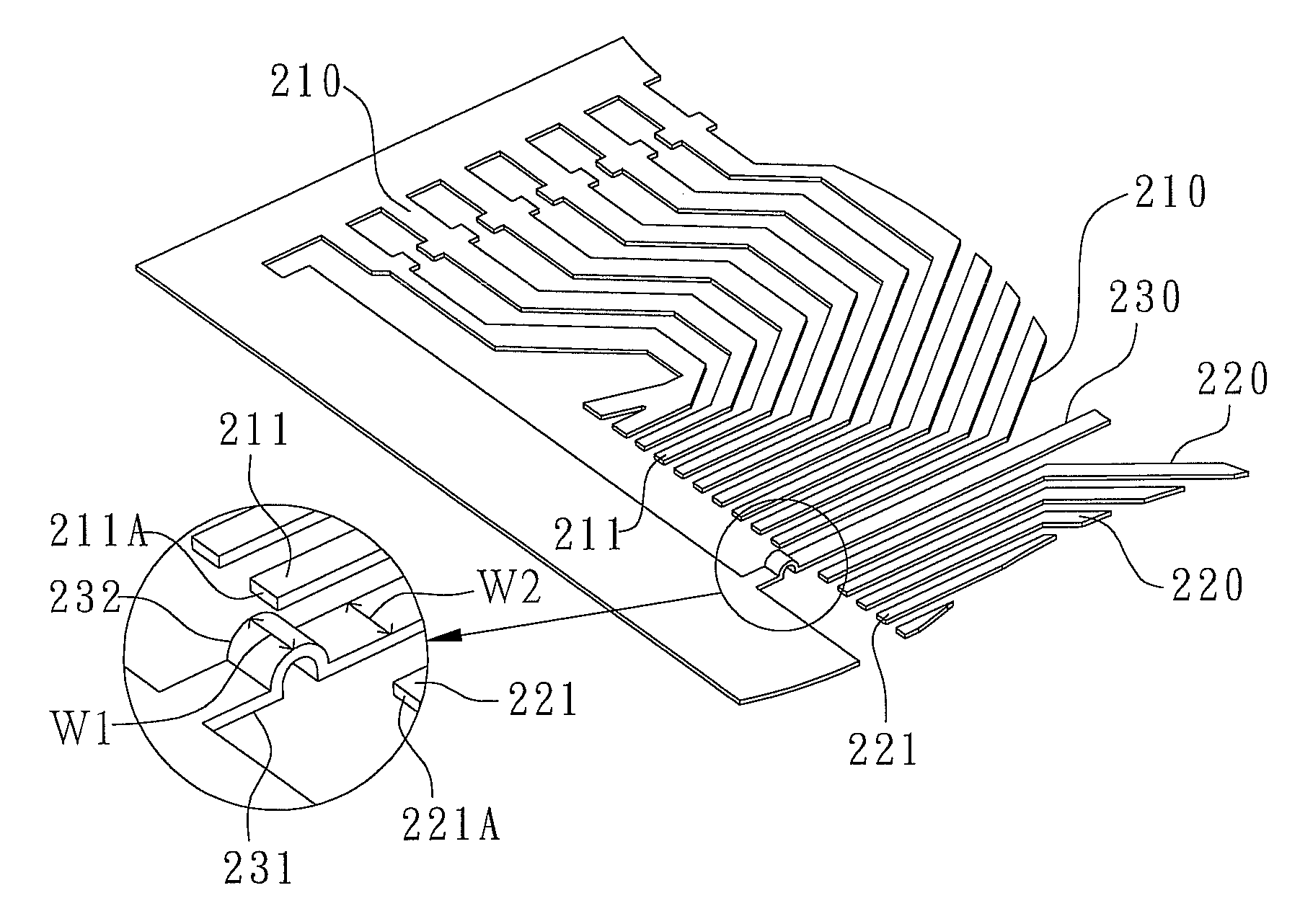
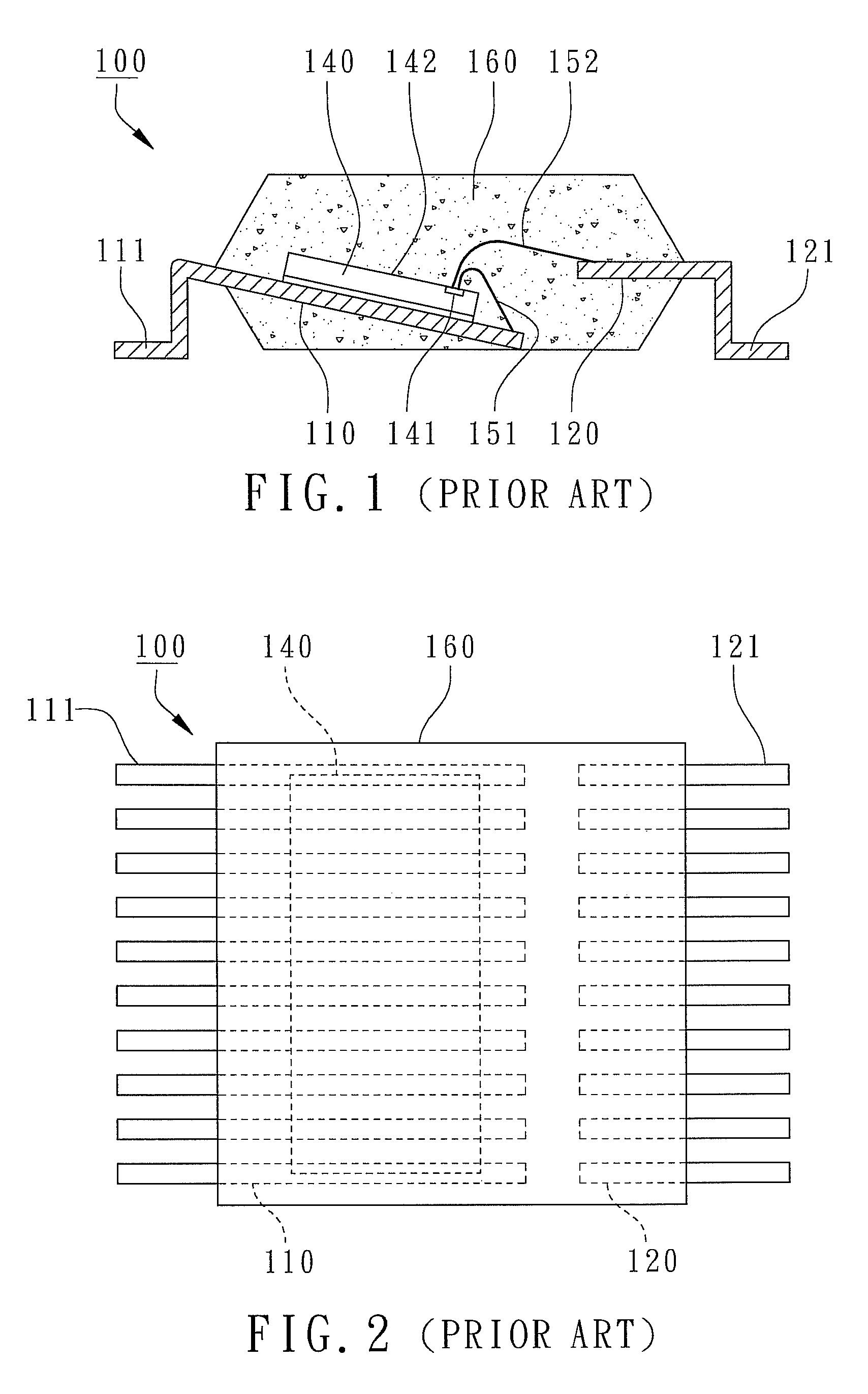
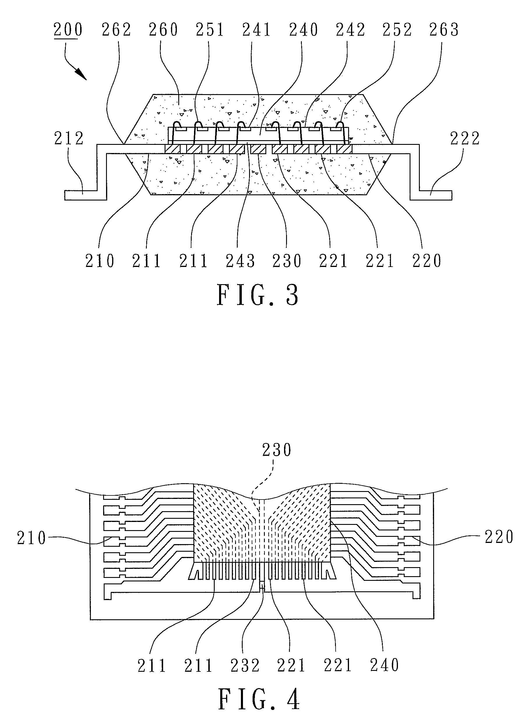
[0019]According to the preferred embodiment of the present invention, a leadframe-based semiconductor package and a leadframe for the package are revealed. As shown in FIG. 3 and FIG. 4, the semiconductor package 200 primarily comprises one or more first leads 210, one or more second leads 220, a supporting bar 230, a chip 240, a plurality of first bonding wires 251, a plurality of second bonding wires 252, and an encapsulant 260. The semiconductor package 200 is a Chip-On-Lead (COL) package.

[0020]As shown in FIG. 5 and FIG. 6, the first leads 210, the second leads 220, and the supporting bar 230 are parts of the same leadframe with proper thickness (about 0.2 mm thick) and made of the same metal material such as copper, iron or its alloy. Each first lead 210 has a first bonding finger 211 and each second lead 220 has a second bonding finger 221. The supporting bar 230 is di...


PUM


Abstract

A leadframe-based semiconductor package and a leadframe for the package are revealed. The semiconductor package primarily includes parts of the leadframe including one or more first leads, one or more second leads, and a supporting bar disposed between the first leads and the second leads and further includes a chip attached to the first leads, the second leads and the supporting bar, a plurality of bonding wires and an encapsulant. The supporting bar has an extended portion projecting from the first bonding finger and the second bonding finger and connected to a non-lead side of the encapsulant wherein the extended portion has an arched bend to absorb the pulling stresses and to block stress transmission. Cracks caused by delamination of the supporting bar will not be created during trimming the supporting bar along the non-lead side of the encapsulant. Moisture penetration along the cracks of the supporting bar to the die-bonding plane under the chip is desirably prevented.

Description

FIELD OF THE INVENTION[0001]The present invention relates to semiconductor packages, especially to leadframe-based semiconductor packages and leadframes for semiconductor packages.BACKGROUND OF THE INVENTION[0002]Even though printed circuit boards and other substrates have gradually replaced leadframes as chip carriers of semiconductor packages, however, leadframe-based semiconductor packages still have the advantages of lower cost and high reliability. One of the leadframe-based semiconductor packages is Chip-On-Lead (COL) semiconductor package. The backside of semiconductor chip is disposed on a plurality of leads of a leadframe. Then the chip is electrically connected to the fingers of the leads by a plurality of bonding wires formed by wire bonding. Finally, an encapsulant is formed by molding to encapsulate the chip and the bonding wires where the external leads of the leads exposed and extended from the sides of the encapsulant are used as the external electrical connections. ...

Claims


Application Information

Patent Timeline
Patent Type & Authority Patents(United States)
IPC IPC(8): H01L23/48H01L23/495H01L23/52
CPCH01L23/3107H01L23/4951H01L23/49551H01L24/48H01L2224/32245H01L2224/48091H01L24/49H01L2224/48257H01L2224/49175H01L2224/73265H01L2924/14H01L2924/1815H01L2224/48247H01L2924/00014H01L2924/00H01L2924/181
Inventor WANG, CHIN-FAHSIEH, WAN-JUNGHSU, YU-MEI
Owner POWERTECH TECHNOLOGY
Why Eureka
Try Eureka