
Carrier structure for semiconductor chip and method for manufacturing the same

a carrier structure and semiconductor chip technology, applied in the association of printed circuit non-printed electric components, basic electric elements, solid-state devices, etc., can solve the problems of inability to improve the electric characteristics of higher-frequency and higher-speed operations, the gap between the chip and the carrier board is large, and the shift is inevitable. achieve the effect of simplifying manufacturing processes and improving alignment accuracy

Active Publication Date: 2009-11-17
PHOENIX PRECISION TECH CORP
View PDF3 Cites 9 Cited by
  • Summary
  • Abstract
  • Description
  • Claims
  • Application Information

AI Technical Summary

Benefits of technology

"The present invention provides a method for manufacturing a carrier structure for semiconductor chips that can avoid alignment errors, simplify manufacturing processes, and achieve the goal of fine circuits. The method involves providing a carrier board with a through cavity in which a semiconductor chip is placed and a removable film is used to temporarily fix the chip. An adhesive material is then filled into the gap between the chip and the carrier board to permanently fix the chip. The method also provides a carrier structure with a built-up structure that includes a dielectric layer and conductive elements for connecting to the chip. The carrier structure helps to disperse stress between different materials and reduces the occurrence of delamination."

Problems solved by technology

Although an objective of high quantity pin counts is achieved, it is limited that electric characteristics are unable to be improved in higher-frequency and higher-speed operation due to long pathways of conductive wires.
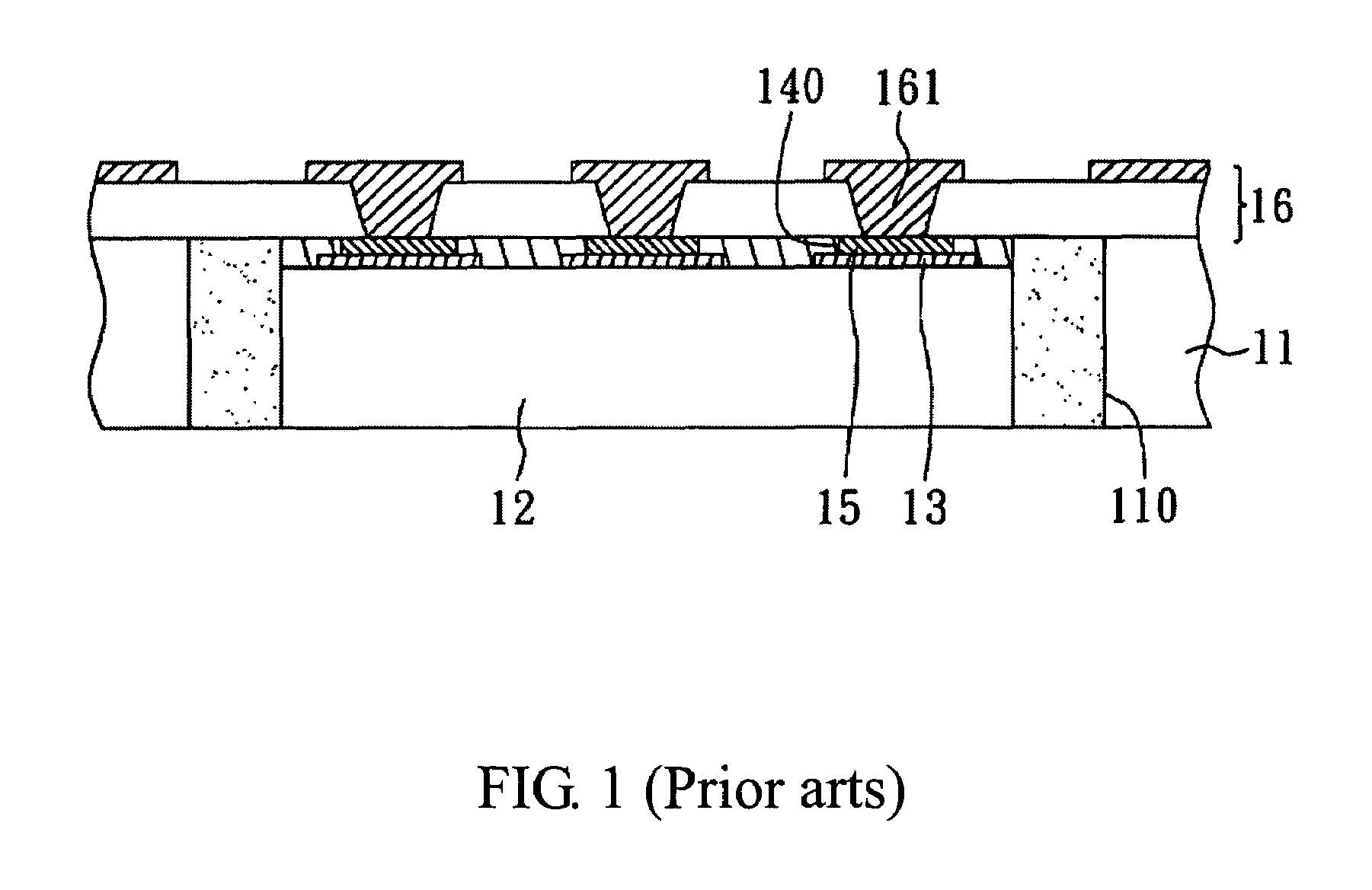
However, a gap exists between the chip and the carrier board.
Prior to fixing the chip, tiny shifts occur inevitably.
Therefore, alignment errors caused by the shifts of the chip are already greater than those resulted from formation of via holes by laser ablation.
Nevertheless, the greater electrode pads of the semiconductor can not satisfy the demand of circuit miniaturization nowadays.
On the other hand, due to aforementioned alignment errors, panels used during manufacturing circuit layer have to be exposed many times in part to control alignment errors being smaller, hence manufacturing processes are difficult to be simplified.
Conclusively, prior arts do not satisfy the requirements of circuit miniaturization, and are not capable of following the trends of compact semiconductor packages.
Furthermore, an adhesive material is required to fill in the gap between the chip and the cavity of the carrier board so that the problem of excess adhesive material spilling out of the gap prior to solidification can occur.
In order to avoid the problem illustrated above, complexity of the manufacturing processes will be unavoidably increased.
Finally, problems of stress between different materials still occur in prior arts to cause warpage, delamination, or popcorn of the carrier board.
Therefore, those problems have become imperative issues to be solved by the industry.

Method used


Image

  • Carrier structure for semiconductor chip and method for manufacturing the same
  • Carrier structure for semiconductor chip and method for manufacturing the same
  • Carrier structure for semiconductor chip and method for manufacturing the same

Examples


embodiment 1

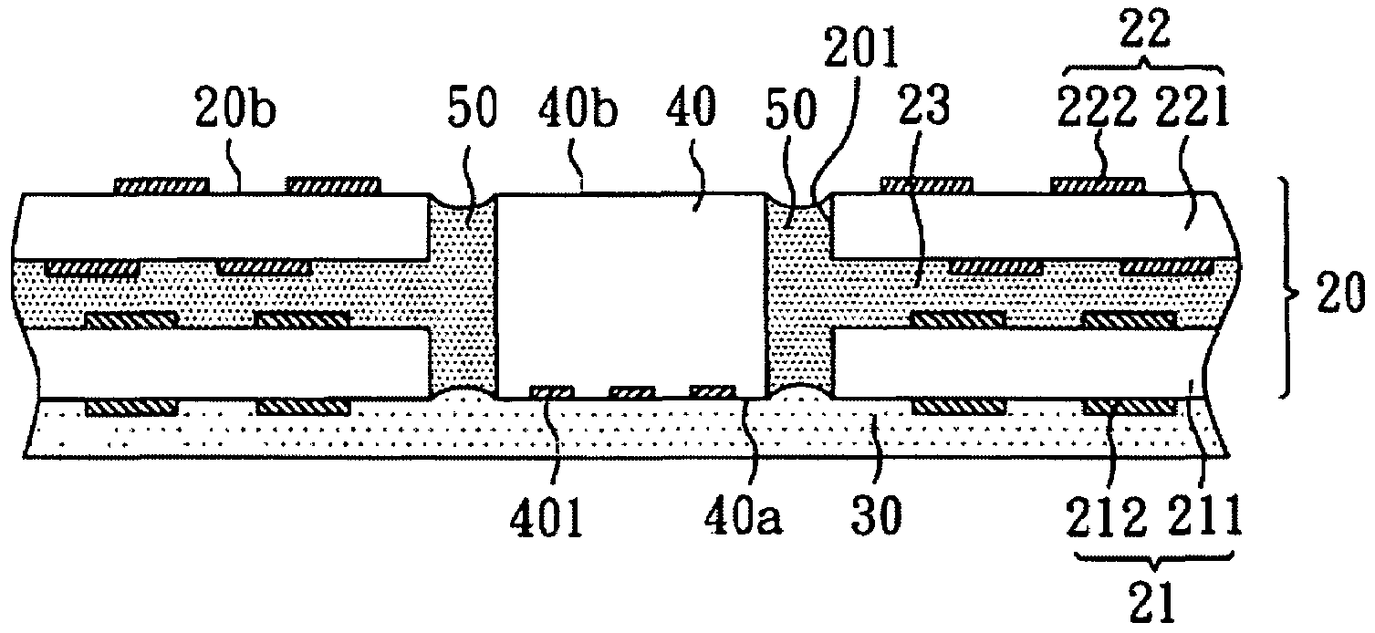
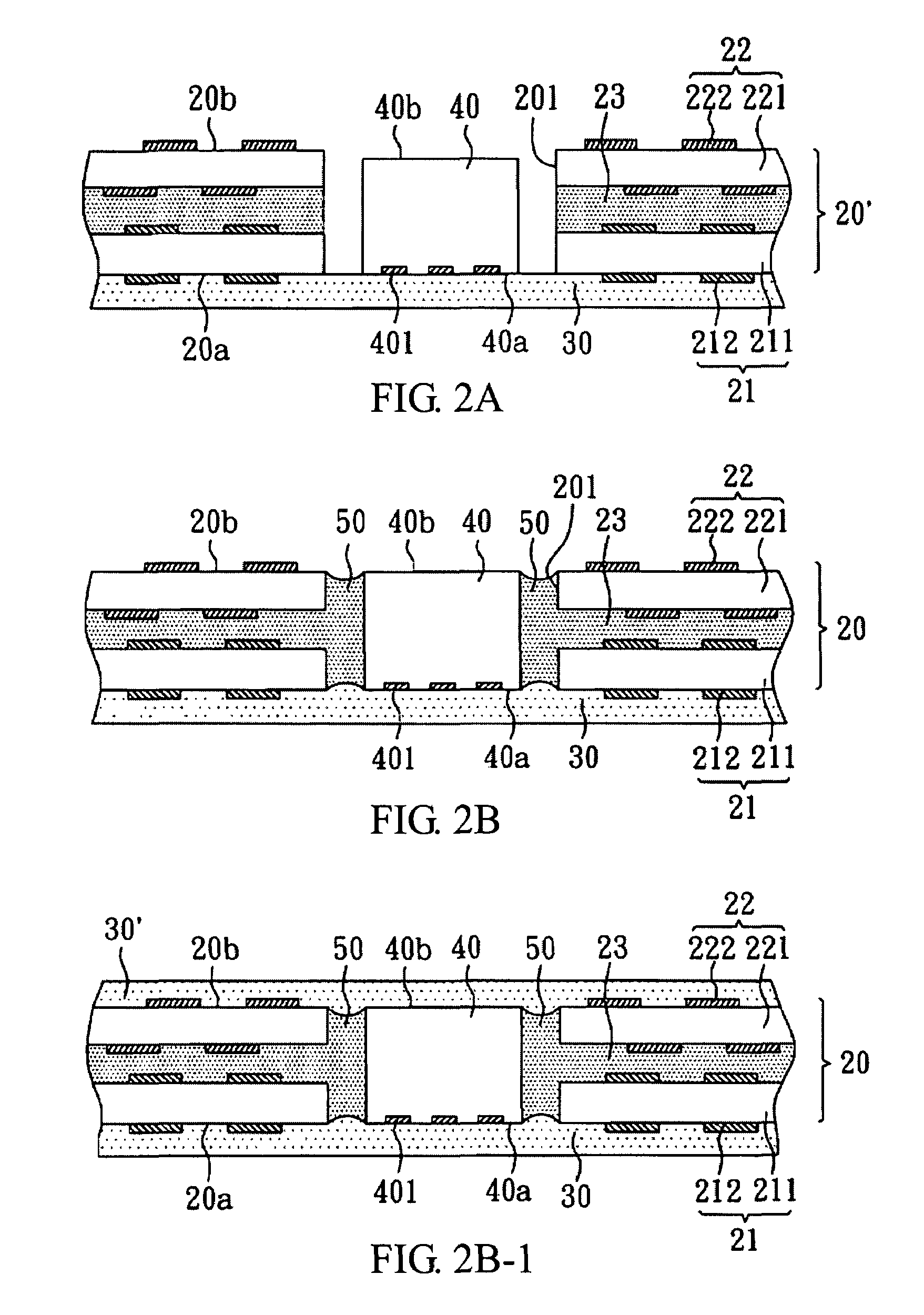
[0032]With reference to FIGS. 2A to 2D, there is shown a flow chart in cross-sectional views for manufacturing a carrier structure for a semiconductor chip in the present invention. As shown in FIG. 2A, a carrier board 20 having a first surface 20a and an opposite second surface 20b is provided. The carrier board 20 has at least one through cavity 201. A semiconductor chip 40 having an active surface 40a and an opposite inactive surface 40b is disposed in the through cavity 201. A first removable film 30 is formed on the first surface 20a of the carrier board 20 so that the semiconductor chip 40 is fixed temporarily by the active surface 40a thereof in the through cavity 201 of the carrier board 20. The carrier board 20 consists of a first core layer 21, a second core layer 22, and an inner adhesive layer 23. The inner adhesive layer 23 is located between the first core layer 21 and the second core layer 22 to form a sandwich structure 20′. The sandwich structure 20′ is manufactured...

embodiment 2

[0039]The present embodiment is approximately similar to Embodiment 1 except for the manufacturing processes of the carrier board 20. With reference to FIGS. 3A and 3B, there is a flow chart in a cross-sectional view. As shown in FIG. 3A, a core layer 21 adhered with a first removable film 30 is provided first. The core layer 21 has a cavity 21a.

[0040]Subsequently, as shown in FIG. 3B, the semiconductor chip 40 is temporarily fixed by the active surface 40a thereof adhered on the first removable film 30 in the cavity 21a of the first core layer 21. Finally, the inner adhesive layer 23 and the second core layer 22 are stacked in sequence on the other surface of the first core layer 21 so as to obtain the structure shown in FIG. 2A. Other steps followed are the same as those of Embodiment 1 hence not to be illustrated again.

embodiment 3

[0041]With reference to FIGS. 4A to 4D, the present embodiment is approximately similar to Embodiment 1 except the inactive surface 40b of the semiconductor chip 40 is higher than the second surface 20b of the carrier board 20 (FIG. 4C). However, in FIG. 2C of Embodiment 1, the inactive surface 40b of the semiconductor chip 40 is flush with the second surface 20b of the carrier board 20. Subsequently, other steps are the same as those of Embodiment 1 hence not to be illustrated again. Likewise, the structure of the present embodiment can be manufactured by the processes disclosed in Embodiment 2.


PUM


Abstract

A carrier structure for a semiconductor chip and a method for manufacturing the same are disclosed. The method includes the following steps: providing a carrier board having at least one through cavity, wherein a removable film is formed on the surface of the carrier board, and a semiconductor chip is temporarily fixed in the through cavity by the removable film; filling the gap between the through cavity of the carrier board and the semiconductor chip with an adhesive material in order to fix the semiconductor chip; and removing the removable film. The disclosed method can reduce the alignment error resulted from the tiny shift of the semiconductor chip caused by jitters before the semiconductor is fixed in the cavity, thereby to increase the accuracy of the alignment, to facilitate fine wiring, and to meet the trend toward compact size of semiconductor packages.

Description

BACKGROUND OF THE INVENTION[0001]1. Field of the Invention[0002]The present invention relates to a carrier structure for a semiconductor chip and a method for manufacturing the same, and especially, to a method for manufacturing a carrier structure having a cavity in which a semiconductor chip is disposed.[0003]2. Description of Related Art[0004]Customer demands of the electronics industry continue to evolve rapidly and the main trends are high integration and miniaturization. In order to satisfy those requirements, especially in the packaging of semiconductor devices, development of packaging substrates sufficing active and passive components and conductive wires has progressed from single layer to multiple layers. This means that a greater usable area is available due to interlayer connection technology.[0005]In the conventional semiconductor device, semiconductor chips are mounted on the front side surface of a substrate by its inactive surface, and then are processed by wire bon...

Claims


Application Information

Patent Timeline
Patent Type & Authority Patents(United States)
IPC IPC(8): H01L23/28H05K1/18
CPCH01L21/568H01L23/3121H01L23/5389H01L24/19H01L2224/04105H01L2924/01033H01L2924/01012H01L2924/01013H01L2924/01029H01L2924/18162H01L2224/20H01L2924/3511H01L2224/96H01L2924/1815
Inventor LIEN, CHUNG-CHENGCHANG, CHIA-WEI
Owner PHOENIX PRECISION TECH CORP
Learn More