
Semiconductor memory device comprising data path controller and related method

a technology of memory device and data path controller, which is applied in the direction of information storage, static storage, digital storage, etc., can solve the problems of difficulty in double the operating speed of memory cell array and corresponding cell core, and achieve the effect of less current consumption, less cost of fabrication, and reduced chip siz

Active Publication Date: 2009-11-24
SAMSUNG ELECTRONICS CO LTD
View PDF8 Cites 0 Cited by
  • Summary
  • Abstract
  • Description
  • Claims
  • Application Information

AI Technical Summary

Benefits of technology

[0018]Embodiments of the invention provide a semiconductor memory device comprising a data output circuit and a related method. The data output circuit may be smaller than a conventional data output circuit, so chip size may be reduced, and the data output circuit may be less expensive to fabricate. In addition, the data output circuit may consume less current than a conventional data output circuit without decreasing data output speed.

Problems solved by technology

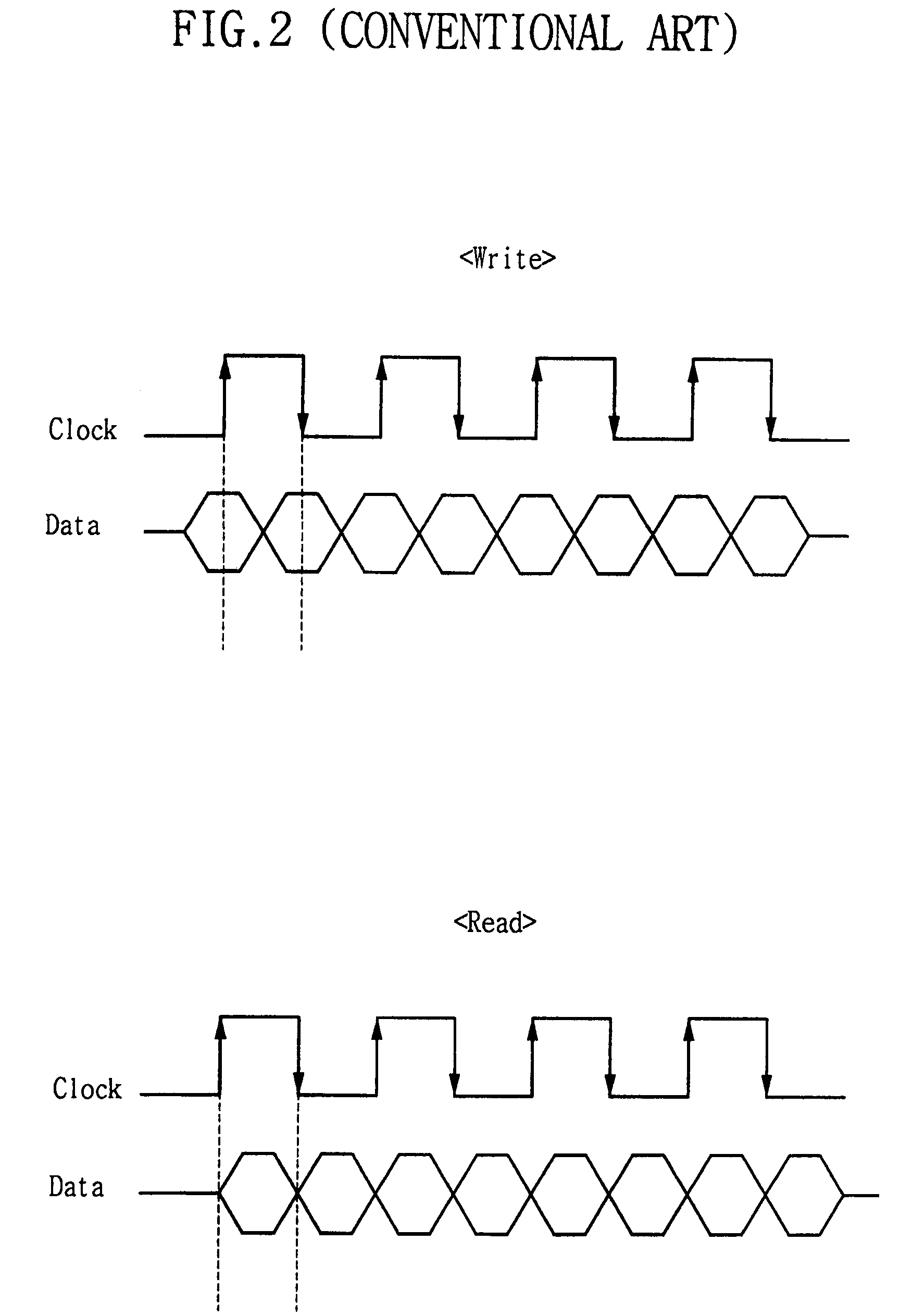
However, it is often difficult to double the operating speed of a memory cell array and a corresponding cell core in order to actually obtain the faster access speeds offered by the DDR DRAM design.

Method used


Image

  • Semiconductor memory device comprising data path controller and related method
  • Semiconductor memory device comprising data path controller and related method
  • Semiconductor memory device comprising data path controller and related method

Examples


Embodiment Construction

[0031]A detailed description of conventional circuits, dynamic random access memory (DRAM), announcing methods, and data output procedures will be omitted here. Throughout the drawings, like reference symbols indicate like or similar elements.

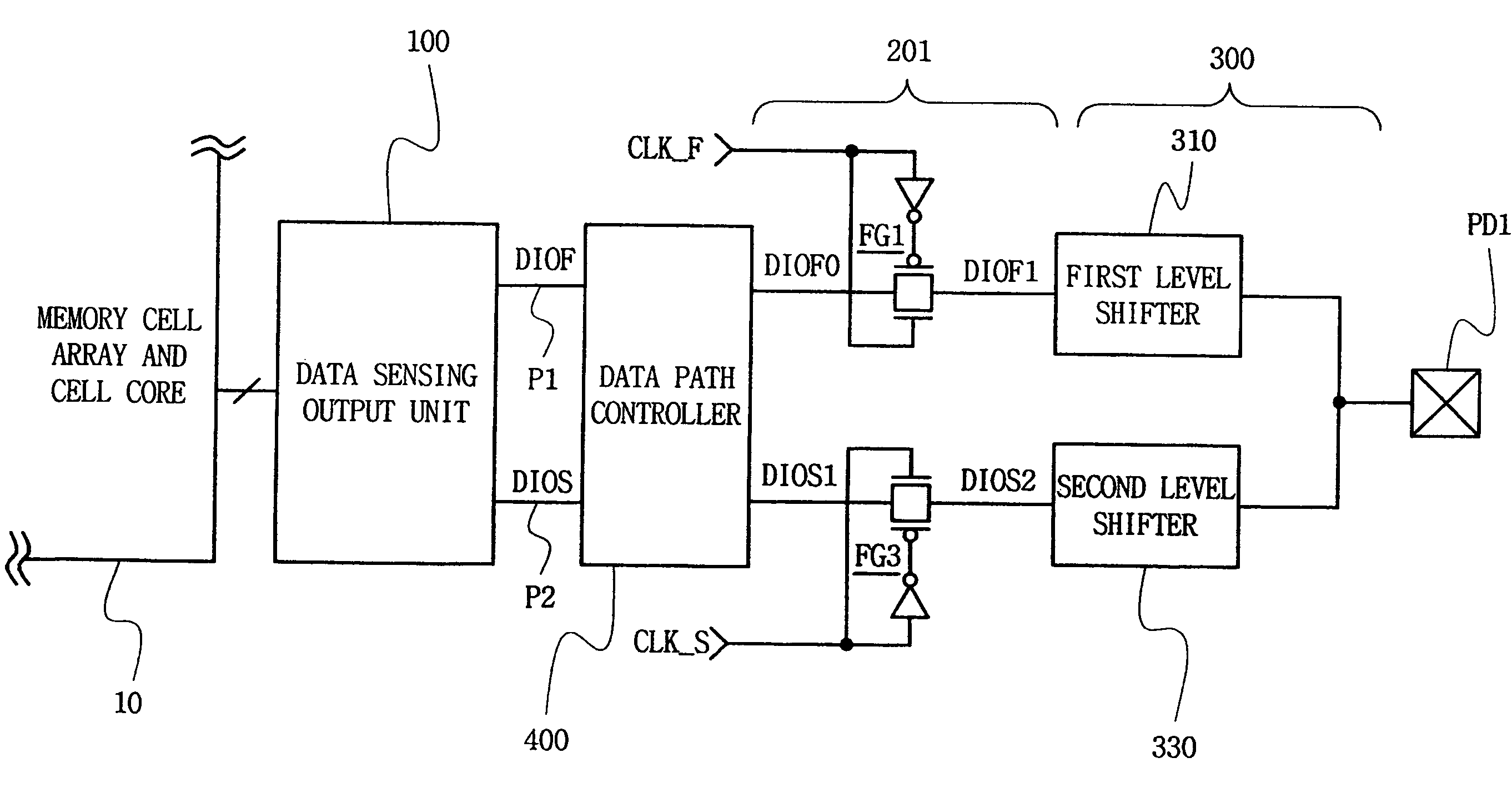
[0032]FIG. 5 illustrates a data path of a data output circuit in accordance with an embodiment of the invention. The data path of the data output circuit of FIG. 5 is similar to that of FIG. 3, and FIG. 5 highlights a data path of a data output circuit. The data path of FIG. 5 corresponds to one input / output pad PD1 (i.e., output terminal PD1) and the data output circuit of FIG. 5 is part of a double data rate (DDR) semiconductor memory device.

[0033]Referring to FIG. 5, a memory cell array and cell core 10 may correspond to a cell array and cell core of a conventional DRAM device. A unit memory cell of the memory cell array may be a DRAM memory cell comprising an access transistor and a storage capacitor. The cell core comprises a conventional ...


PUM


Abstract

A semiconductor memory device and a related method are disclosed. The semiconductor memory device includes a data sensing output unit simultaneously providing first and second data to first and second data path lines, respectively; and a data output circuit, wherein the first and second data are serially output to an output terminal through the data output circuit. The device further includes a data transmitter operationally connecting the first data path line to the data output circuit and operationally connecting the second data path line to the data output circuit; and a data path controller connected between the data sensing output unit and the data transmitter, delaying the second data, and including first and second delay elements, wherein each of the first and second delay elements is disposed along one of the first and second data path lines.

Description

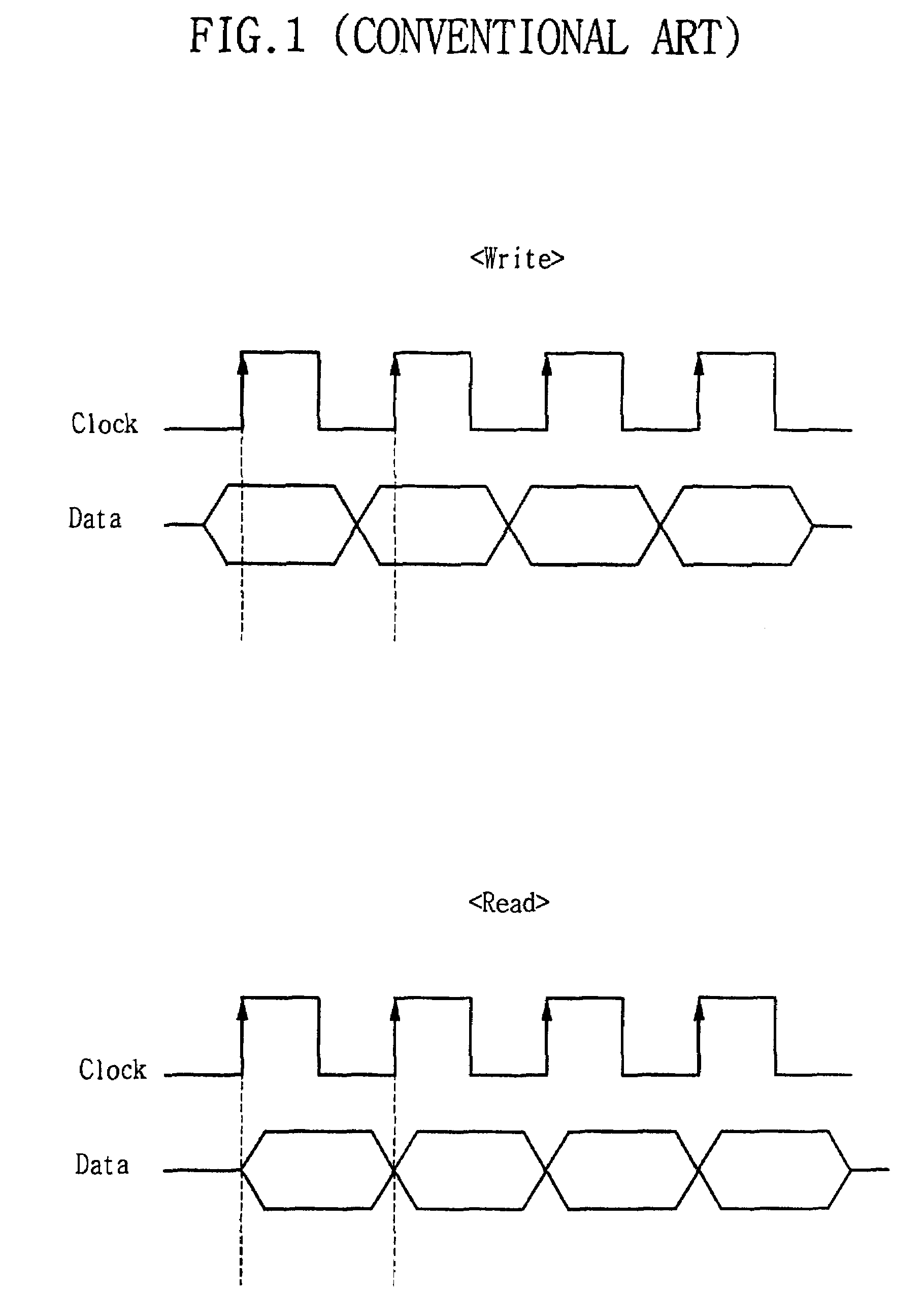
BACKGROUND OF THE INVENTION[0001]1. Field of the Invention[0002]Embodiments of the invention relate to a semiconductor memory device and a related method. In particular, embodiments of the invention relate to a semiconductor memory device comprising a data path controller and a related method.[0003]This application claims priority to Korean Patent Application 10-2006-0079424, filed on Aug. 22, 2006, the subject matter of which is hereby incorporated by reference in its entirety.[0004]2. Description of the Related Art[0005]The accuracy, speed, and corresponding bandwidth of data transmissions between contemporary central processing units (CPUs) and associated semiconductor memory devices are increasingly important to the proper operation of incorporating products.[0006]In this regard, there are several types of Dynamic Random Access Memory (DRAM) devices commonly used with CPUs. One type is the single data rate (SDR) DRAM. A SDR DRAM accesses data in response to the rising edge of a ...

Claims


Application Information

Patent Timeline
Patent Type & Authority Patents(United States)
IPC IPC(8): G11C8/16
CPCG11C7/1048G11C7/1051G11C7/1066G11C11/4096G11C7/22G11C11/4076G11C7/1069G11C2207/2254G11C2207/2227G11C2207/105
Inventor JEONG, WOO-PYO
Owner SAMSUNG ELECTRONICS CO LTD
Learn More