Photo-sensor array for motion detection

a technology of motion detection and photosensor array, which is applied in the field of imaging systems, can solve the problems of requiring twice the number of capacitors, consuming less power, and storing an image, so as to reduce the required circuit area, reduce errors, and consume less power

Inactive Publication Date: 2005-06-16
MICROSOFT TECH LICENSING LLC
View PDF14 Cites 0 Cited by
  • Summary
  • Abstract
  • Description
  • Claims
  • Application Information

AI Technical Summary

Benefits of technology

[0010] An image sensor according to the present invention addresses many of the problems of prior art imaging systems such as shown in FIG. 1 and as described above. In the context of motion sensing, high resolution images are less critical than speed and reduction of errors caused by unpredictable variations among individual imaging elements. The present invention permits a reduction of such errors, and at the same time allows a reduction in required circuit area. The present invention further allows construction of imaging arrays that consume less power and are less expensive to fabricate.

Problems solved by technology

However, this scheme requires twice the number of capacitors to store the image.
This architecture is also susceptible to parasitic signal couplings, capacitor mismatch, capacitor leakages and charge injections, and can only store an image for a relatively short time without degradation of the image data.
Moreover, this architecture presents problems with regard to digitally-oriented Application Specific Integrated Circuit (ASIC) technologies, which may involve high sub-threshold leakages and low power supply voltages.
Although it is possible to implement multiple ADCs and other digital circuitry components to parallel process multiple pixels, the multiple components required for parallel processing must have matched properties, which further increases cost.
Such parallel processing also increases overall power consumption and die size.
However, these alternative configurations are generally not well suited for motion detection applications in compact devices (such as, e.g., computer input devices), particularly when power consumption is a concern.
Moreover, many of these alternative photosensor array configurations draw significant power.
Although high power consumption may be acceptable when there are relatively long intervals between images, and when multiple other processing functions are not required, high power consumption can be particularly disadvantageous in motion detection devices.
While excessive power consumption is generally undesirable, it is especially so when a battery supplies power.
Electronic photography configurations also present problems in scaling an array to a smaller size.
In order to obtain a highly detailed image, numerous circuit components are necessary, and such components require space.
As indicated, many of the problems with known alternative imaging designs result, at least in part, from attempts to increase image resolution.
To date, however, no known imaging system has attempted to balance the degree of pixel-level circuit components needed for accurate motion detection images with the simplicity necessary for rapid, low power operation in a compact size.

Method used


Image

  • Photo-sensor array for motion detection
  • Photo-sensor array for motion detection
  • Photo-sensor array for motion detection

Examples


Embodiment Construction

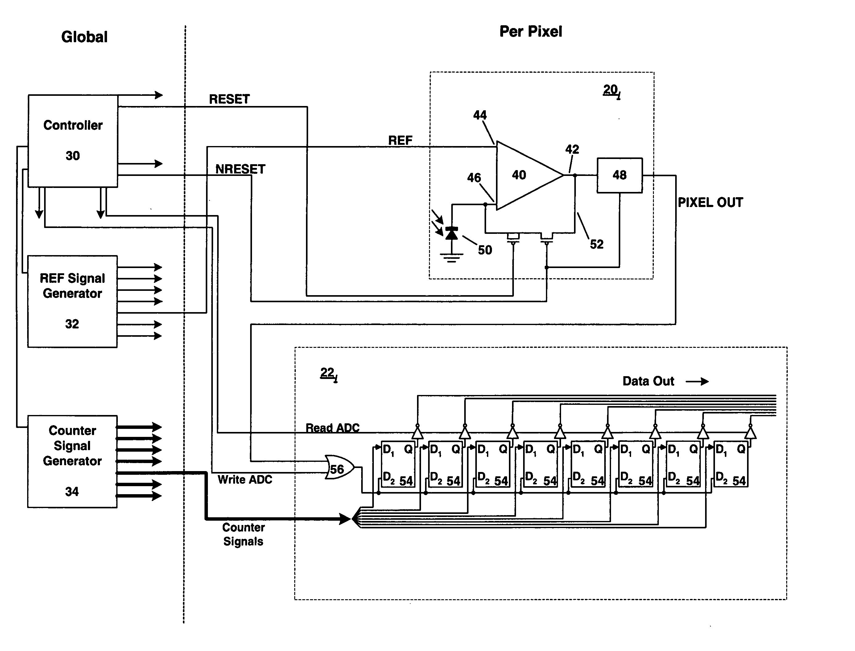
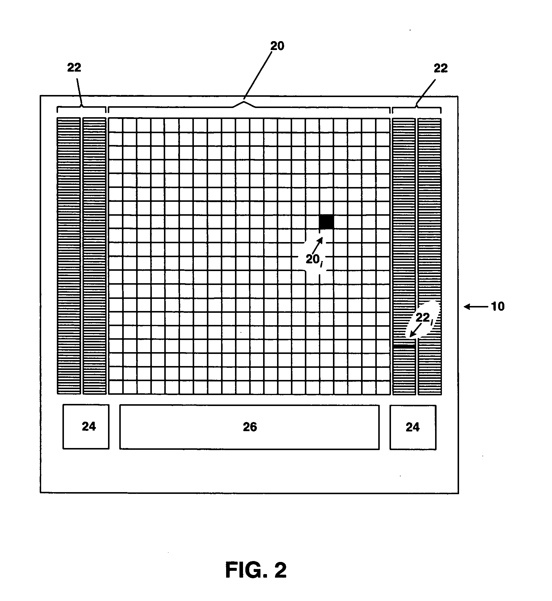
[0021]FIG. 2 is a block diagram of an Integrated Circuit (IC) 10 forming (or forming part of) an image sensor according to one embodiment of the invention. IC 10 includes an array of pixels 20. Located on either side of pixel array 20 are storage elements 22. In one preferred embodiment, a separate storage element corresponds to each pixel. In other words, there is a one-to-one correspondence between pixels and storage elements. Additional circuitry may also be located on IC 10. In the example of FIG. 2, counters, address decoders and other circuitry may be located in regions 24. Similarly, biasing circuitry and Digital to Analog Conversion (DAC) circuitry may be located in region 26. Other circuitry may also be located on IC 10, and the depicted circuitry could be rearranged and / or located on other ICs or circuit boards.

[0022] In operation, array 20 may be positioned to receive light reflected from a surface or object and thereby generate an image of the surface or object. IC 10 i...


PUM


Abstract

Pixels in an array of image sensor pixels contain photo-sensors and circuits having inputs connected to the photosensors. The circuits have feedback loops for reducing fixed pattern noise in the array. Output from each pixel is used to latch a multibit counter value supplied by a global counter. Each feedback loop preferably includes a pair of alternately-toggling switching transistors to minimize unwanted charge injection. An image sensor according to the invention can be used for, e.g., motion sensing.

Description

CROSS-REFERENCE TO RELATED APPLICATIONS [0001] This application is a continuation of U.S. patent application Ser. No. 10 / 305,062, filed Nov. 27, 2002 and titled “Photo-Sensor Array for Motion Detection,” now U.S. Pat. No. ______. Said application is hereby incorporated by reference in its entirety.FIELD OF THE INVENTION [0002] This invention relates to imaging systems having arrays of photo-sensors and associated storage elements, and more specifically, to an array photo-sensors having offset cancellation circuitry within each pixel. BACKGROUND OF THE INVENTION [0003] Photo-sensitive electronic components can be used to create electronic imaging systems, including systems for detecting and measuring motion. One application for motion detection is a computer pointing or input device, such as a computer mouse. Use of electronic imaging for such purposes is described in, e.g., U.S. Pat. Nos. 6,303,924 (titled “Image Sensing Operator Input Device”) and 6,172,354 (titled “Operator Input ...

Claims


Application Information

Patent Timeline
Patent Type & Authority Applications(United States)
IPC IPC(8): H01L27/00H01L27/146
CPCH01L27/14643
Inventor KNEE, DEREK L.OLIVER, THOMAS C.RENSBERGER, GARY M.
Owner MICROSOFT TECH LICENSING LLC
Why Eureka
Try Eureka