Fabrication of hybrid substrate with defect trapping zone

a hybrid substrate and defect trapping technology, applied in the direction of basic electric elements, semiconductor/solid-state device manufacturing, electric devices, etc., can solve the problem that the layer is liable to modify the electrical properties of the final structure, and achieve the effect of reducing the cost of production

Active Publication Date: 2009-12-15
SOITEC SA
View PDF11 Cites 26 Cited by
  • Summary
  • Abstract
  • Description
  • Claims
  • Application Information

AI Technical Summary

Benefits of technology

[0027]The present invention provides a process for fabricating a hybrid substrate that prevents the formation of defects on the surface of the semiconductor active layer transferred, and more precisely defects due to the build-up of gaseous elements at the various bonding interfaces of the substrate. In one particular embodiment, such a process must also be applicable to the fabrication of a hybrid substrate whose active layer has a small thickness, i.e. less than 400 nm, and whose insulator layer is less than 5 nm, or even nonexistent.
[0029]For this purpose, the invention relates to a process for fabricating a hybrid substrate that can be used in the fields of optics, electronics or optoelectronics. This process comprises providing a first insulator layer on a first substrate of semiconductor material, the layer having an exposed surface; forming a roughened surface on the first insulator layer; providing a second insulator layer of semiconductor material on the roughened surface of the first insulator layer to form a trapping zone at an interface between the layers; bonding a second substrate onto the second insulator layer by molecular adhesion, wherein one of the substrates includes a zone of weakness therein formed by implantation of atomic species and defining an active layer; and transferring the active layer by detachment at the zone of weakness to form the hybrid substrate. Advantageously, the roughened surface of the first substrate forms a trapping zone that is capable of retaining gaseous atomic species present at the interface of the layers to reduce formation of defects on the surface of the active layer that is transferred.

Problems solved by technology

The reason for this is that such layers are liable to modify the electrical properties of the final structure.

Method used


Image

  • Fabrication of hybrid substrate with defect trapping zone
  • Fabrication of hybrid substrate with defect trapping zone
  • Fabrication of hybrid substrate with defect trapping zone

Examples


first embodiment

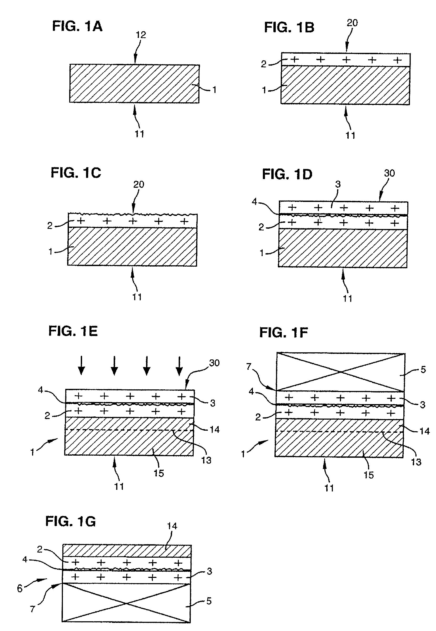
[0064]the process according to the invention will now be described with reference to FIGS. 1A to 1G.

[0065]FIG. 1A shows a substrate 1 called a “donor” substrate, as this is the one which provides the active layer in the hybrid substrate to be obtained.

[0066]The donor substrate 1 has two opposed faces 11 and 12, called “rear” and “front” faces respectively. It may be a monolayer or multilayer substrate. As an example of a multilayer donor substrate, it is possible to use a bulk substrate coated with an epitaxially grown layer, such as a bulk silicon substrate coated with an epitaxially grown germanium layer.

[0067]The donor substrate 1 consists at least partly of a semiconductor material, more precisely one of those commonly used in the electronics field, especially silicon. The donor substrate 1 may also be, for example, made of germanium (Ge), gallium nitride (GaN), gallium arsenide (GaAs) or silicon-germanium (SiGe). As shown in FIG. 1B, a first insulator layer 2 is then formed or ...

second embodiment

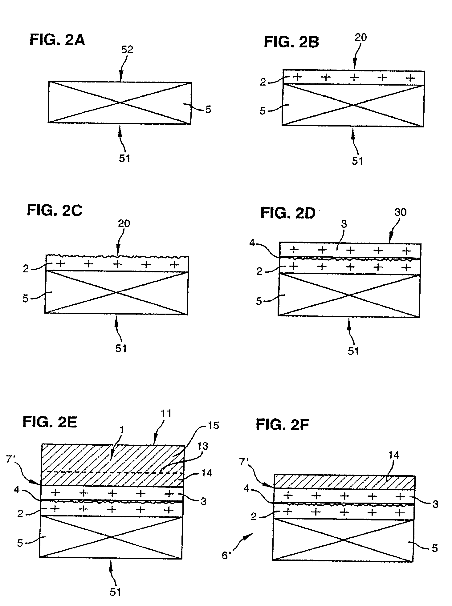
[0089]A second embodiment will now be described with reference to FIGS. 2A to 2F. According to this embodiment, the successive insulator layers 2 and 3 are deposited on the front face of the receiver substrate 5 instead of the front face of the donor substrate 1. The rear and front faces of the substrate 5 bear the references 51 and 52 respectively. The choice of insulating materials constituting the layers 2 and 3 and the techniques for forming or depositing the layers 2 and 3 are identical to those described above. The same applies to the roughening techniques. The same elements bear the same numerical references.

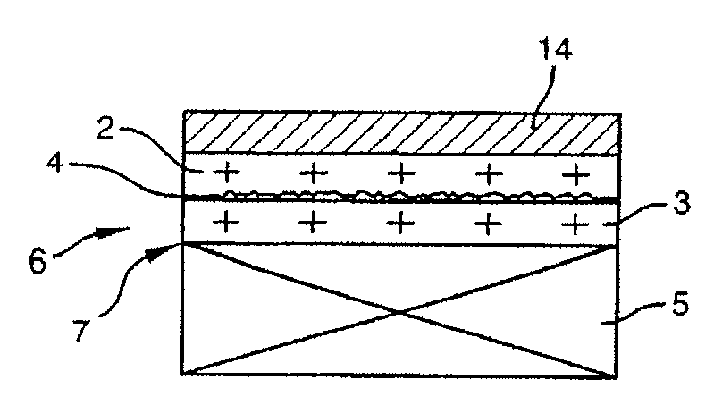
[0090]FIG. 2E shows that the source substrate 1 has undergone the step of atomic species implantation, allowing the zone of weakness 13 to be formed, before being bonded by molecular adhesion onto the insulator layer 3. To do this, the source substrate 1 may optionally be temporarily covered with an oxide layer making it easier to implement the aforementioned SMART-CUT® p...


PUM


Abstract

A process for fabricating a hybrid substrate that has a defect trapping zone. The process includes the steps of forming or depositing a first insulator layer on a first substrate of semiconductor material; increasing roughness of the first insulator layer surface; depositing a second insulator layer on the roughened surface of the first insulator to form a trapping zone between the layers; bonding a second substrate onto the second insulator layer by molecular adhesion; and transferring an active layer formed by the implantation of atomic species into one of the substrates. The trapping zone is able to retain gaseous species present at the various interfaces of the hybrid substrate to limit the formation of defects on the surface of the active layer that is transferred.

Description

BACKGROUND[0001]The present invention relates to a process for fabricating a hybrid substrate that can be used in the field of optics, electronics or optoelectronics. The terms “optics”, “electronics” and “optoelectronics” in general include microelectronics, nano-electronics, micro-optoelectronics, nano-optoelectronics and components technology.[0002]A hybrid substrate is a substrate comprising at least two layers of material of the same or different nature, the term “nature” covering both the chemical nature of the material and its physicochemical properties and / or its crystalline orientation. Among these hybrid substrates are in particular those known by the acronym “SeOI”, which stands for “Semiconductor On Insulator”. Such a substrate comprises an insulator layer, for example made of oxide, buried between a generally thin layer of semiconductor material, the “active” layer, and a bulk substrate or “receiver” substrate made of semiconductor material.[0003]In the rest of the desc...

Claims


Application Information

Patent Timeline
Patent Type & Authority Patents(United States)
IPC IPC(8): H01L21/30H01L21/46
CPCH01L21/76254
Inventor HEBRAS, XAVIER
Owner SOITEC SA
Why Eureka
Try Eureka