Semiconductor laser device and manufacturing method thereof

a laser device and semiconductor technology, applied in semiconductor lasers, laser details, electrical devices, etc., can solve the problems difficult to maximize the characteristics of each laser element, and increasing the amount of wavelength shifts, so as to achieve the effect of increasing the number of diffusion steps

Active Publication Date: 2009-12-15
PANASONIC SEMICON SOLUTIONS CO LTD
View PDF4 Cites 2 Cited by
  • Summary
  • Abstract
  • Description
  • Claims
  • Application Information

AI Technical Summary

Benefits of technology

[0019]According to the structure of the semiconductor laser device of the invention, impurities are less likely to be piled up in the first semiconductor laser element having the AlGaAs-based first active layer. This can suppress reduction in wavelength shift caused by the impurity pileup and contamination with In, whereby COD degradation is less likely to occur in the first semiconductor laser element. Moreover, equalization of the composition proceeds efficiently in the semiconductor laser element having the AlGaInP-based second active layer, whereby wavelength shift can be increased. Accordingly, both outputs of the first semiconductor laser element and the second semiconductor laser element can be improved. Moreover, the impurity diffusion rate is lower in an AlGaAs-based material than in an AlGaInP-based material. Therefore, in the case where the end face window structures are formed by impurity diffusion, the lower end of the second end face window structure can be easily made to be located lower than the lower end of the first end face window structure by controlling the thickness of the second contact layer. As a result, a high-power, low-cost monolithic multi-wavelength semiconductor laser device can be implemented.
[0021]According to the method for manufacturing a semiconductor device of the invention, the distance from the lower end of the first active layer to the lower end of the first end face window structure can easily be made shorter than the distance from the lower end of the second active layer to the lower end of the second end face window structure without increasing the number of diffusion steps. Accordingly, a high-power, low-cost monolithic multi-wavelength semiconductor laser device can be implemented.

Problems solved by technology

However, the monolithic dual-wavelength semiconductor laser device has a problem that it is difficult to maximize characteristics of each laser element.
Excessive impurity diffusion causes pileup of impurities in the active layer.
On the other hand, in a red laser element having an active layer made of an AlGaInP-based material, problems such as reduction in wavelength shift amount as in the infrared laser element does not occur when the cladding layer is made of AlGaInP.
However, if impurity diffusion reaches a GaAs (gallium arsenide) buffer layer beyond the AlGaInP-based cladding layer, a leakage current is generated and characteristics of the semiconductor laser are degraded.
Therefore, when the infrared laser element and the red laser element are individually formed with heat history in the monolithic dual-wavelength semiconductor laser device, excessive impurity diffusion may occur in the laser gain portion, which may result in reduction in reliability.

Method used


Image

  • Semiconductor laser device and manufacturing method thereof
  • Semiconductor laser device and manufacturing method thereof
  • Semiconductor laser device and manufacturing method thereof

Examples


first embodiment

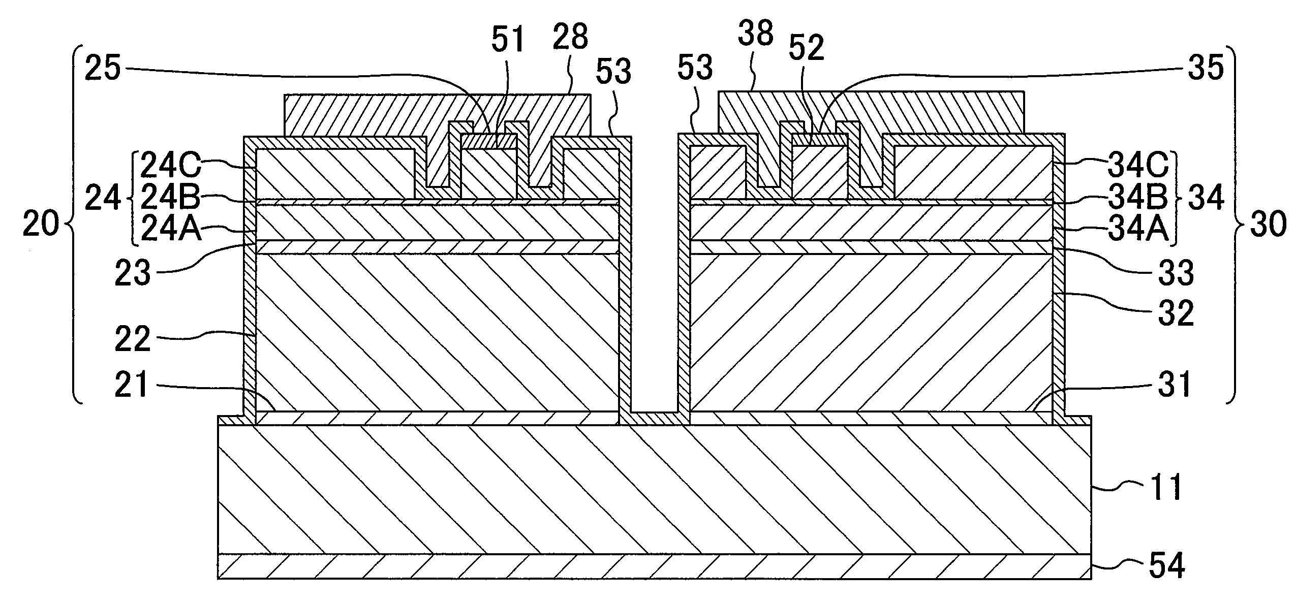
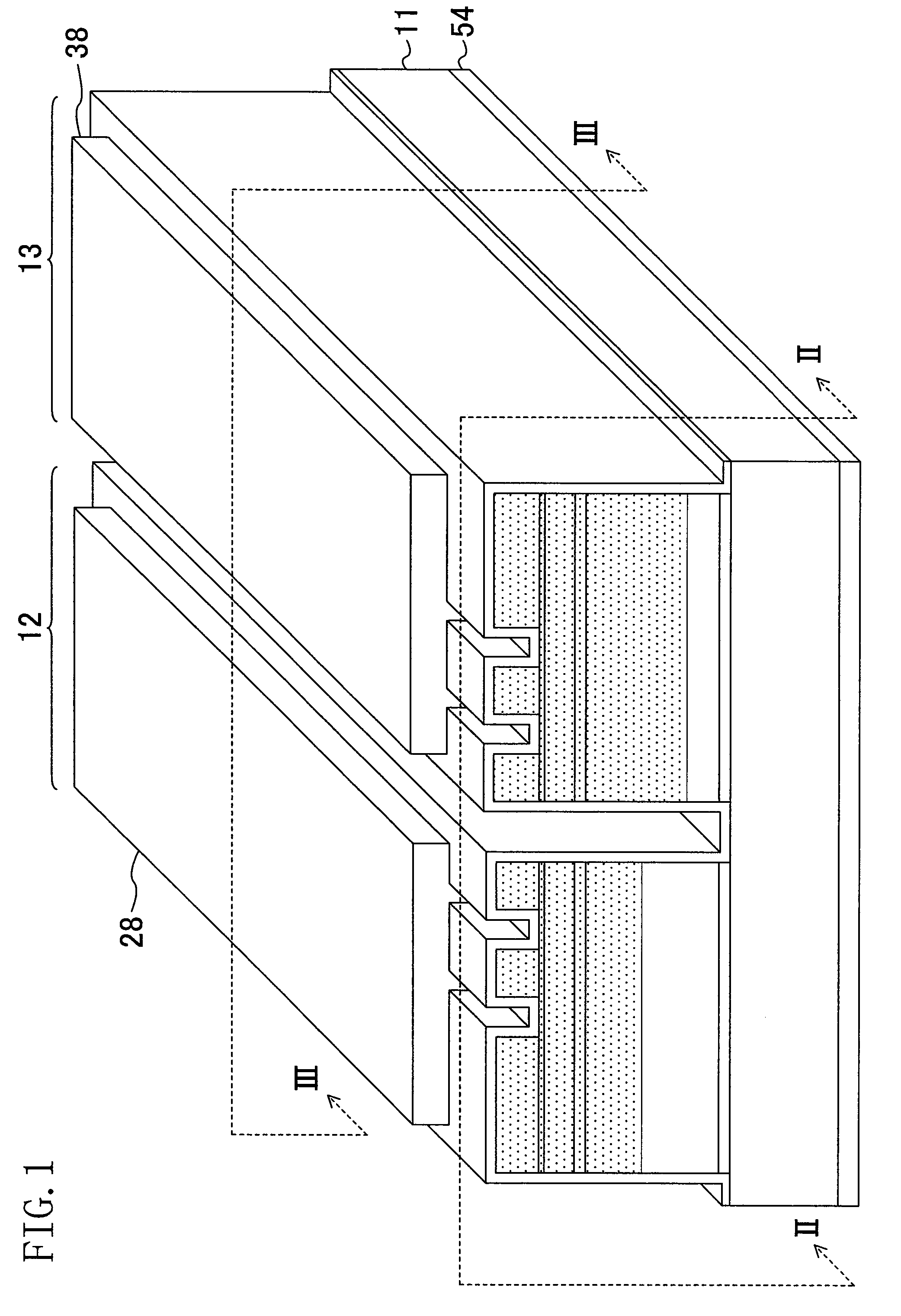
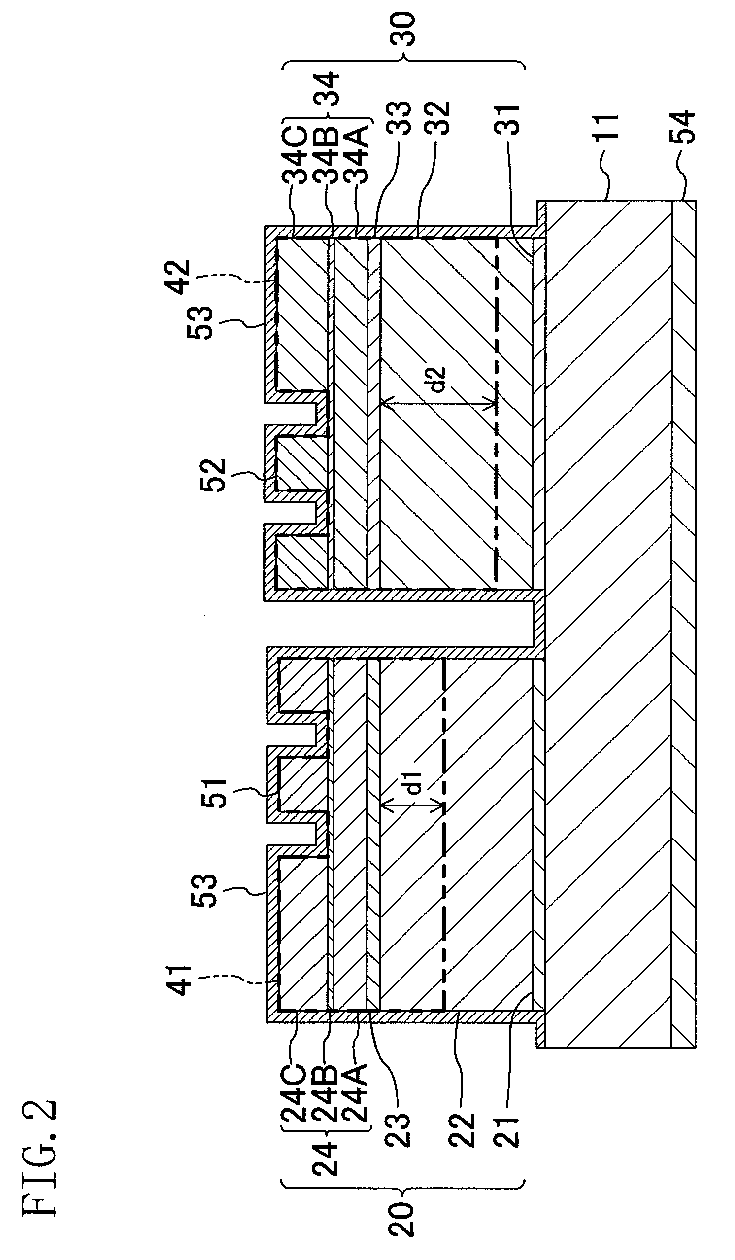
[0046]Hereinafter, a first embodiment of the invention will be described with reference to the figures. FIG. 1 shows a structure of a semiconductor laser device according to the first embodiment. FIG. 2 shows a structure of a cross section (a window region) taken along line II-II in FIG. 1, and FIG. 3 shows a structure of a cross section (a gain region) taken along line III-III in FIG. 1.

[0047]As shown in FIGS. 1 through 3, the semiconductor laser device of this embodiment is a monolithic dual-wavelength semiconductor laser device including an infrared laser element 12 and a red laser element 13 which are formed on an n-type GaAs (gallium arsenide) semiconductor substrate 11.

[0048]The infrared laser element 12 has a first semiconductor layer 20. The first semiconductor layer 20 includes a first buffer layer 21, a first n-type cladding layer 22, a first active layer 23, a first p-type cladding layer 24, and a first contact layer 25 which are sequentially formed on the semiconductor s...

second embodiment

[0082]Hereinafter, a second embodiment of the invention will be described with reference to the figures. FIG. 14 shows a structure of a semiconductor laser device according to the second embodiment. FIG. 15 shows a cross-sectional structure taken along line XV-XV in FIG. 14, and FIG. 16 shows a cross-sectional structure taken along line XVI-XVI in FIG. 14. In FIGS. 14 through 16, the same elements as those in FIGS. 1 through 3 are denoted with the same reference numerals and characters, and description thereof will be omitted.

[0083]In the semiconductor laser device of the second embodiment, the lower end of the first end face window structure 41 of the infrared laser element 12 does not reach the lower end of the first n-type cladding layer 22, and the lower end of the second end face window structure 42 of the red laser element 13 reaches the lower end of the second n-type cladding layer 32.

[0084]In the semiconductor laser device of this embodiment, the composition of the second bu...

third embodiment

[0093]Hereinafter, a third embodiment of the invention will be described with reference to the figures. FIG. 18 shows a structure of a semiconductor laser device according to the third embodiment. FIG. 19 shows a cross-sectional structure taken along line XIX-XIX in FIG. 18, and FIG. 20 shows a cross-sectional structure taken along line XX-XX in FIG. 18. In FIGS. 18 through 20, the same elements as those of FIGS. 1 through 3 are denoted with the same reference numerals and characters, and description thereof will be omitted.

[0094]In the semiconductor laser device of the third embodiment, the lower end of the first end face window structure 41 of the infrared laser element 12 does not reach the lower end of the first n-type cladding layer 22, and the lower end of the second end face window structure 42 of the red laser element 13 reaches the lower end of the second n-type cladding layer 32. The first end face window structure 41 is formed below the first etch stop layer 24B.

[0095]In ...


PUM


Abstract

A semiconductor laser device includes a first semiconductor laser element and a second semiconductor laser element. The first semiconductor laser element has a first end face window structure that is a region including first impurities formed near an end face, and the second semiconductor laser element has a second end face window structure that is a region including second impurities formed near an end face. The distance from a lower end of a first active layer to a lower end of the first end face window structure is shorter than the distance from a lower end of a second active layer to a lower end of the second end face window structure.

Description

CROSS REFERENCE TO RELATED APPLICATION[0001]This application claims priority under 35 U.S.C. §119 on Patent Application No. 2007-244068 filed in Japan on Sep. 20, 2007, the entire contents of which are hereby incorporated by reference.BACKGROUND OF THE INVENTION[0002]1. Field of the Invention[0003]The invention generally relates to a semiconductor laser device and a manufacturing method thereof. More particularly, the invention relates to a monolithic semiconductor laser device for emitting laser light of a plurality of wavelengths and a manufacturing method thereof.[0004]2. Background Art[0005]A semiconductor laser device is used as a pickup light source of an optical disc device and a light source for optical information processing, optical communication and optical measurement. For example, an infrared laser device having a 780 nm (nanometer) wavelength band is used as a pickup light source for playing back and recording CDs (Compact Discs) and MDs (Mini Discs). A red laser devic...

Claims


Application Information

Patent Timeline
Patent Type & Authority Patents(United States)
IPC IPC(8): H01S5/00
CPCB82Y20/00H01S5/162H01S5/4031H01S5/22H01S2301/173H01S5/34326H01S5/4087H01S5/34313
Inventor KASHIMA, TAKAYUKIMAKITA, KOUJIYOSHIKAWA, KENJI
Owner PANASONIC SEMICON SOLUTIONS CO LTD
Why Eureka
Try Eureka