Semiconductor chip and method of fabricating the same
a semiconductor chip and fuse technology, applied in the direction of semiconductor/solid-state device details, diodes, semiconductor devices, etc., can solve the problems of reducing the processing increasing the number of fuses to be blown, and needing more time for blowing fuses, so as to shorten the process time of blowing fuses and efficiently fabricate semiconductor chips. , the effect of shortening the fabrication tim
- Summary
- Abstract
- Description
- Claims
- Application Information
AI Technical Summary
Benefits of technology
Problems solved by technology
Method used
Image

Examples
first embodiment
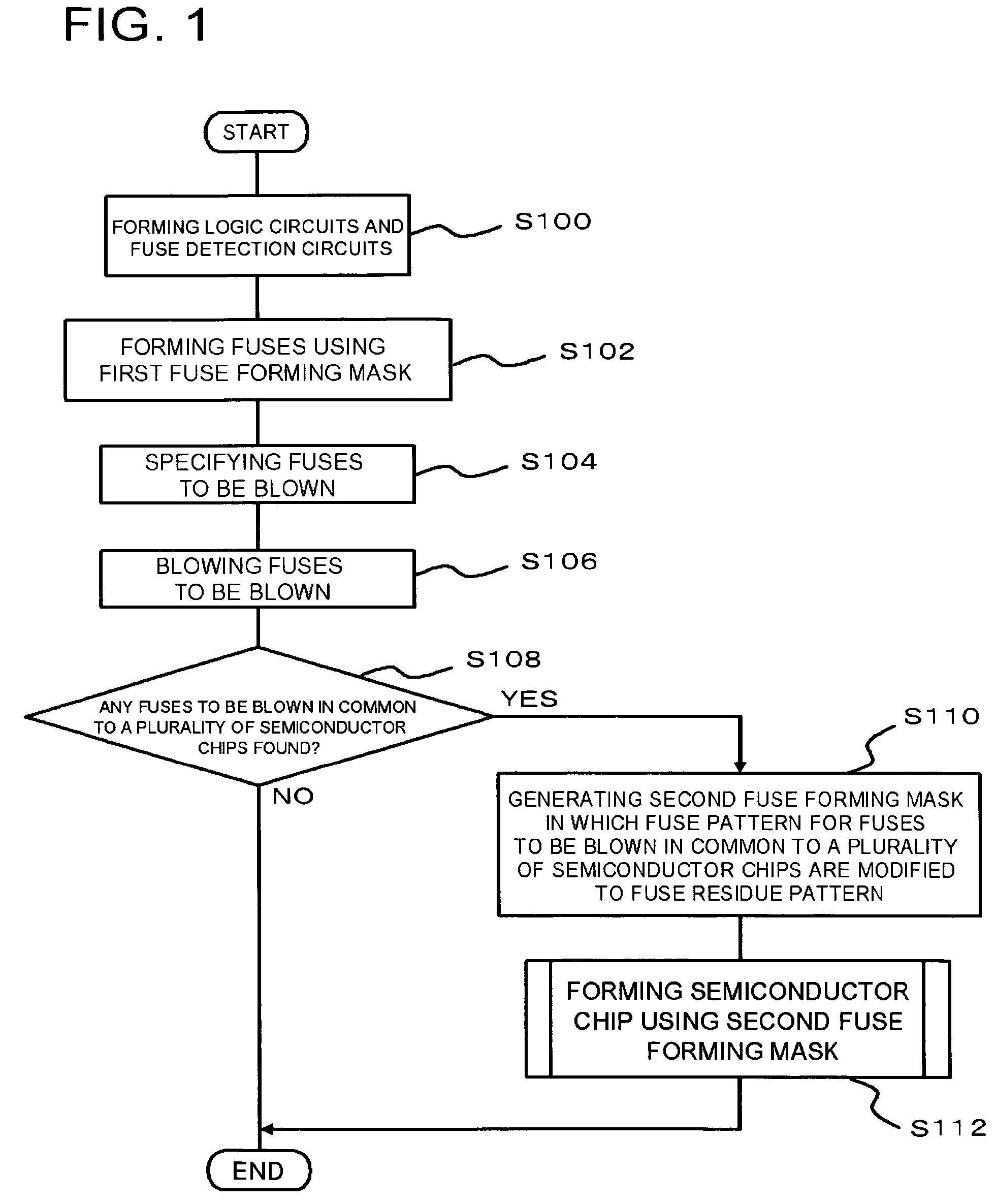
[0079]The first embodiment will be described exemplifying a fuse used for regulating voltage between two logic circuits.
[0080]FIG. 3 is a top view showing a configuration of the first fuse-forming mask used in step S102 in FIG. 1.
[0081]The first fuse-forming mask 220 has a plurality of fuse patterns 132 formed thereon. Each fuse pattern 132 includes a first terminal pattern 134, a blowable region pattern 136, and a second terminal pattern 138. The fuse pattern 132 may have other various geometries, without being limited to the geometry shown herein.
[0082]FIG. 4 is a schematic top view showing a configuration of the first semiconductor chip 200 formed by using the first fuse-forming mask 220 shown in FIG. 3.
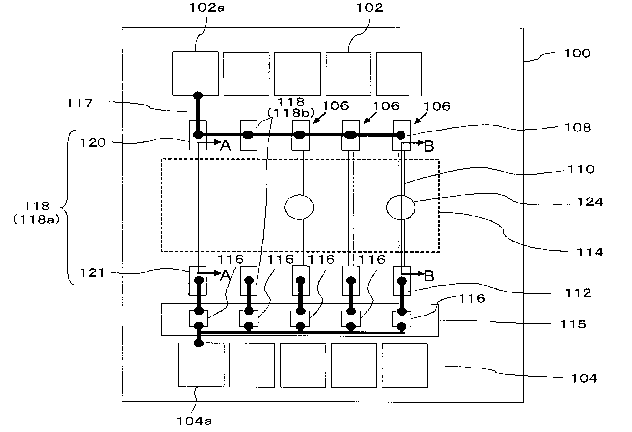
[0083]The first semiconductor chip 200 includes a plurality of fuses 106. Each fuse 106 includes a first terminal 108, a second terminal 112, and a blowable region 110 electrically connected thereto and disposed therebetween. In the first embodiment, blowable regions 110 of the fu...
second embodiment
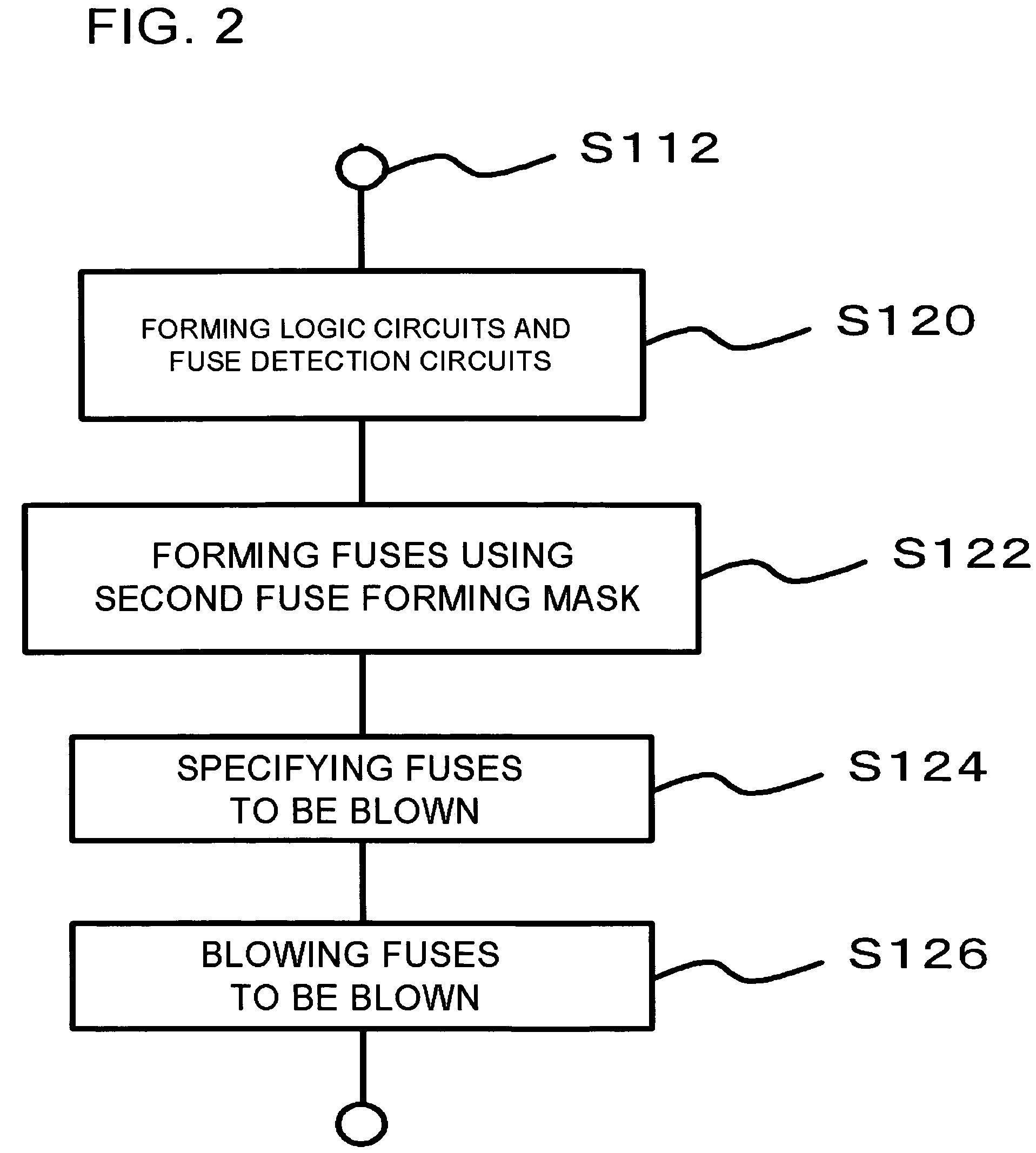
[0124]Also in the second embodiment, fuses regulating voltage between two logic circuits will be described similarly to as in the first embodiment. In the second embodiment, the geometry of the fuse residues 118 differ from that in the first embodiment.
[0125]FIG. 12 is a top view showing a configuration of the second fuse-forming mask 130 in the second embodiment.
[0126]The first fuse residue pattern 141 of the fuse residue pattern 140 in the second embodiment has, in addition to a pattern same as that of the first terminal pattern 134 of the fuse pattern 132, a pattern same as that of a part of the blowable region pattern 136. The second fuse residue pattern 142 of the fuse residue pattern 140 has, in addition to a pattern same as that of the second terminal pattern 138 of the fuse pattern 132, a pattern same as that of a part of the blowable region pattern 136. The first fuse residue pattern 141 and the second fuse residue pattern 142 herein are not connected to each other.
[0127]FI...
third embodiment
[0135]Also in the third embodiment, fuses regulating voltage between two logic circuits will be described similarly to as in the first and second embodiments. The third embodiment differs from the first embodiment and the second embodiment, in that the fuses 106 are blown by current supply.
[0136]FIG. 16 is a schematic top view showing a configuration of the second semiconductor chip 100 in which the fuses 106 to be blown are blown by current supply, rather than laser irradiation.
[0137]In the third embodiment, the second semiconductor chip 100 further includes a current generation circuit 119. The target fuses 106 can be blown by being supplied with current generated by the current generation circuit 119.
[0138]FIG. 17 is a sectional view taken along line D-D in FIG. 16.
[0139]In the third embodiment, there is no need of forming the fuse blowing recess 114 to the second insulating film 156 and the polyimide film 158. The blowable region 110 can electrically be disconnected by the blow ...
PUM
 Abstract
Description
Claims
Application Information
 - R&D
- Intellectual Property
- Life Sciences
- Materials
- Tech Scout
- Unparalleled Data Quality
- Higher Quality Content
- 60% Fewer Hallucinations
Browse by: Latest US Patents, China's latest patents, Technical Efficacy Thesaurus, Application Domain, Technology Topic, Popular Technical Reports.
© 2025 PatSnap. All rights reserved.Legal|Privacy policy|Modern Slavery Act Transparency Statement|Sitemap|About US| Contact US: help@patsnap.com