

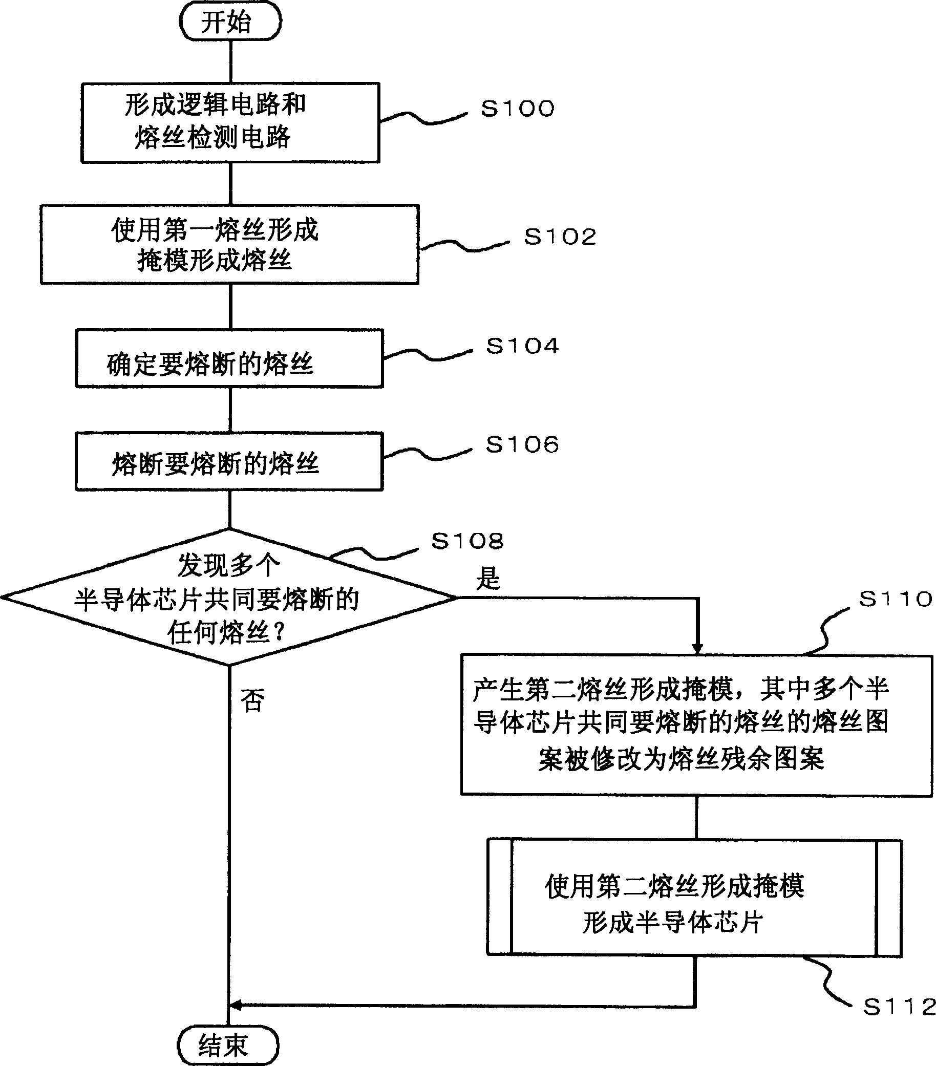
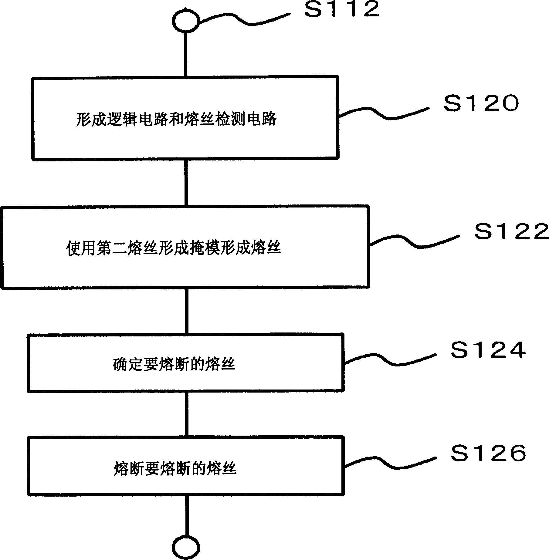
Semiconductor chip and method of fabricating the same
一种半导体、芯片的技术,应用在半导体/固态器件制造、半导体器件、半导体/固态器件零部件等方向,能够解决增加TAT等问题,达到缩短TAT、缩短处理时间、防止侵入及空隙的产生的效果
- Summary
- Abstract
- Description
- Claims
- Application Information
AI Technical Summary
Problems solved by technology
Method used
Image

Examples
no. 1 example
[0078] The first embodiment will be described to exemplify a fuse for adjusting voltage between logic circuits.
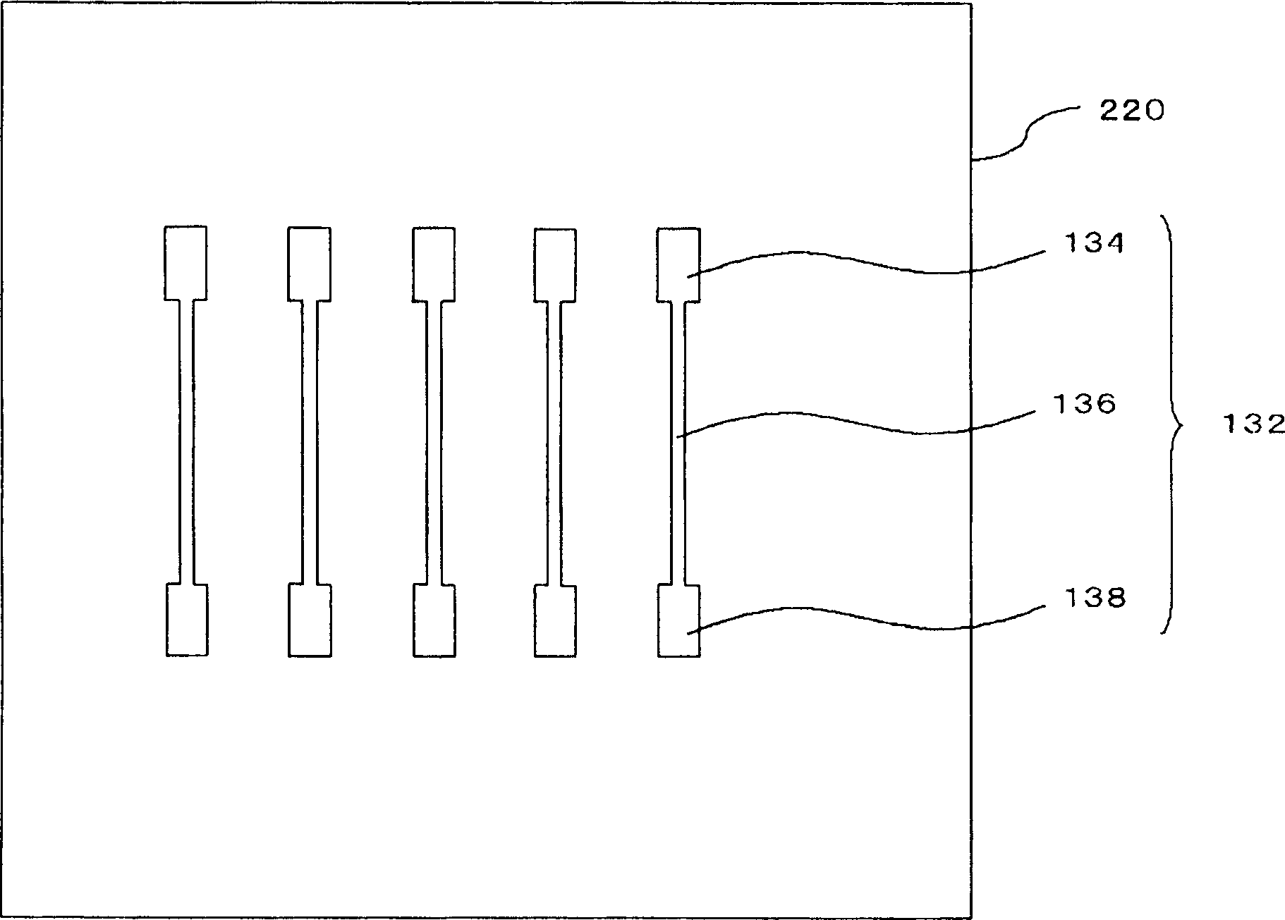
[0079] image 3 is shown in figure 1 A top view of the construction of the first fuse formation mask used in step 102.
[0080] The first fuse forming mask 220 has a plurality of fuse patterns 132 formed thereon. Each fuse pattern 132 includes a first terminal pattern 134 , a fusing area pattern 136 and a second terminal pattern 138 . The fuse pattern 132 may have other different geometries and is not limited to the geometries shown here.
[0081] Figure 4 is shown by using image 3 A top view of the configuration of the first semiconductor chip 200 formed by the first fuse forming mask 220 is shown.
[0082] The first semiconductor chip 200 includes a plurality of fuses 106 . Each fuse 106 includes a first terminal 108 , a second terminal 112 and a fusible region 110 electrically connected to and disposed between the first terminal 108 and the second termi...
no. 2 example
[0124] In the second embodiment, a fuse that adjusts a voltage between two logic circuits is described similarly to that in the first embodiment. In the second embodiment, the geometry of the fuse remnant 118 is different from that in the first embodiment.
[0125] Figure 12 is a top view showing the configuration of the second fuse forming mask 130 in the second embodiment.
[0126] In the second embodiment, the first fuse remnant pattern 141 of the fuse remnant pattern 140 has the same part as the fusible area pattern 136 in addition to having the same pattern as the first terminal pattern 134 of the fuse pattern 132 . picture of. The second fuse residue pattern 142 of the fuse residue pattern 140 has the same pattern as part of the blowable area pattern 136 in addition to having the same pattern as the second terminal pattern 138 of the fuse pattern 132 . The first fuse remnant pattern 141 and the second fuse remnant pattern 142 are not connected to each other here.
...
no. 3 example
[0136] In the third embodiment, a fuse that adjusts a voltage between two logic circuits is described similarly to that in the first and second embodiments. The third embodiment differs from the first and second embodiments in that the fuse 106 is blown by a current source.
[0137] Figure 16 is a top view showing the configuration of the second semiconductor chip 100 that blows the fuse 106 to be blown by a current source instead of laser irradiation.
[0138] In the third embodiment, the second semiconductor chip 100 further includes a current generation circuit 119 . The target fuse 106 can be blown by supplying the current generated by the current generating circuit 119 .
[0139] Figure 17 is along Figure 16 A cross-sectional view taken along line D-D in .
[0140] In the third embodiment, there is no need to form the fuse blowing groove 114 to the second insulating film 156 and the polyimide film 158 . The fusible region 110 can be electrically disconnected by a...
PUM
 Abstract
Description
Claims
Application Information