Anti-fuse one-time-programmable nonvolatile memory

a non-volatile memory and anti-fuse technology, applied in the field of non-volatile memory cells, can solve the problems of high complex and expensive processes, and insufficient production cost of dprom cells, and achieve the effect of low cos

Inactive Publication Date: 2009-12-29
MACRONIX INT CO LTD
View PDF12 Cites 18 Cited by
  • Summary
  • Abstract
  • Description
  • Claims
  • Application Information

AI Technical Summary

Benefits of technology

[0013]The small size of the anti-fuse OTP nonvolatile memory cell and its simple cell structure result in a compact anti-fuse OTP nonvolatile memory array and low cost for its fabrication process.

Problems solved by technology

Solid-state data storage technologies like EPROM and EEPROM have been optimized for high-speed applications, resulting in complex and expensive processes.
The prior art teaches diode programmable read only memories (DPROMs), however, the fabrication process of such DPROM cells is too complex due to the needs for deep trench isolation and silicon epitaxy layers.
Therefore, the production cost of the DPROM cell is not low enough.

Method used


Image

  • Anti-fuse one-time-programmable nonvolatile memory
  • Anti-fuse one-time-programmable nonvolatile memory
  • Anti-fuse one-time-programmable nonvolatile memory

Examples


Embodiment Construction

[0025]Reference is made in detail to embodiments of the invention. While the invention is described in conjunction with the embodiments, the invention is not intended to be limited by these embodiments. On the contrary, the invention is intended to cover alternatives, modifications and equivalents, which may be included within the spirit and scope of the invention as defined by the appended claims. Furthermore, in the following detailed description of the invention, numerous specific details are set forth in order to provide a thorough understanding of the invention. However, as is obvious to one ordinarily skilled in the art, the invention may be practiced without these specific details. In other instances, well-known methods, procedures, components, and circuits have not been described in detail so that aspects of the invention will not be obscured.

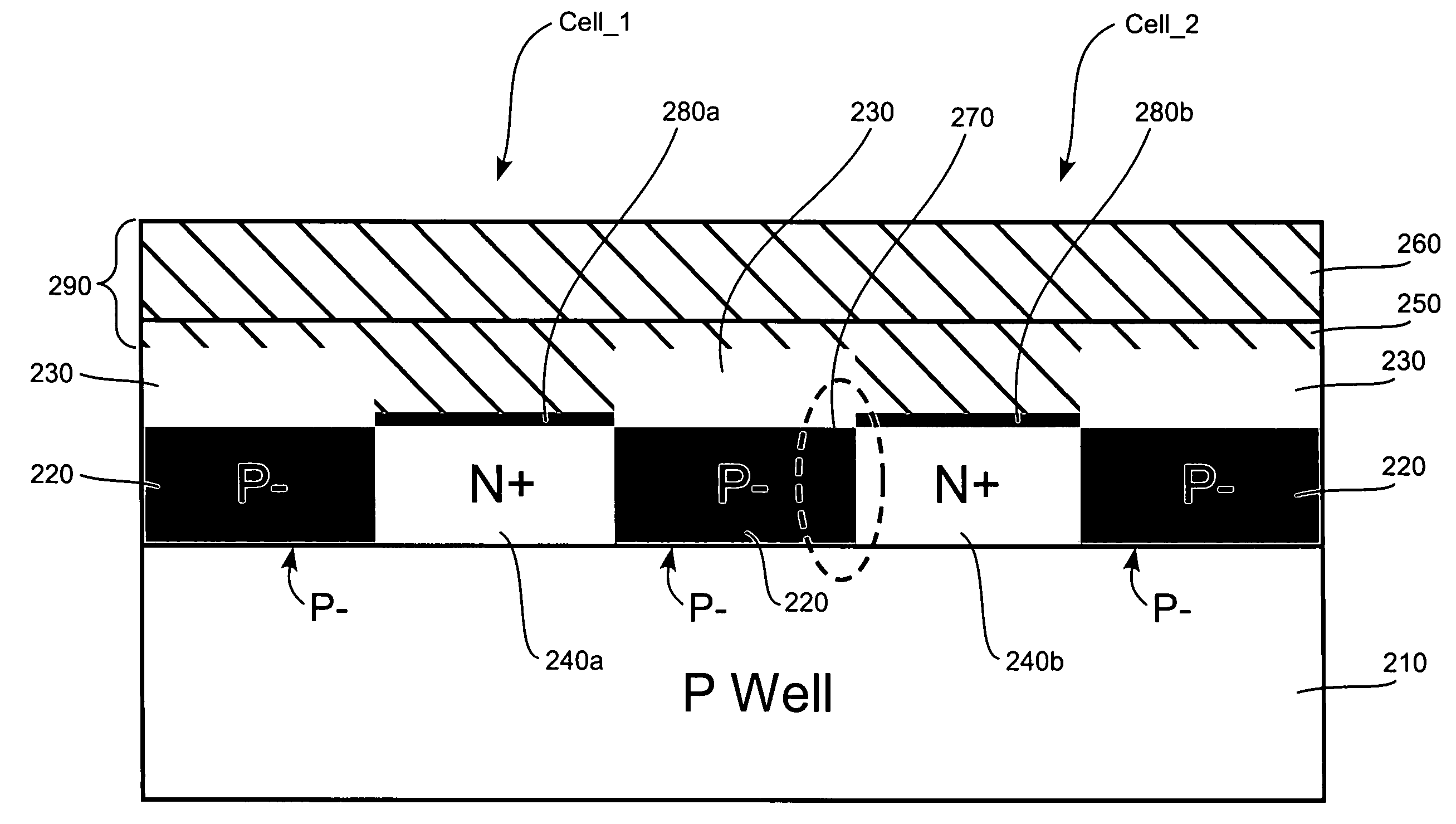
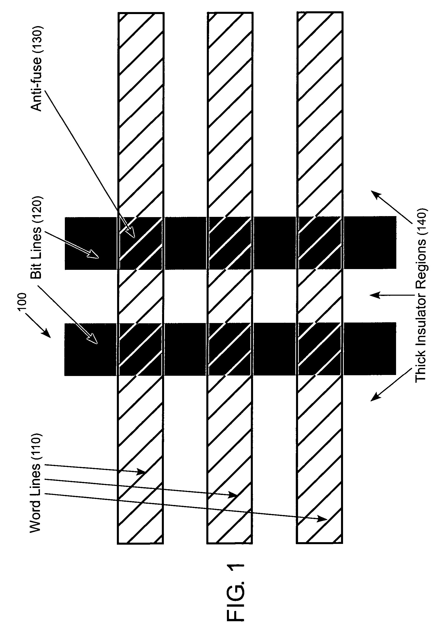
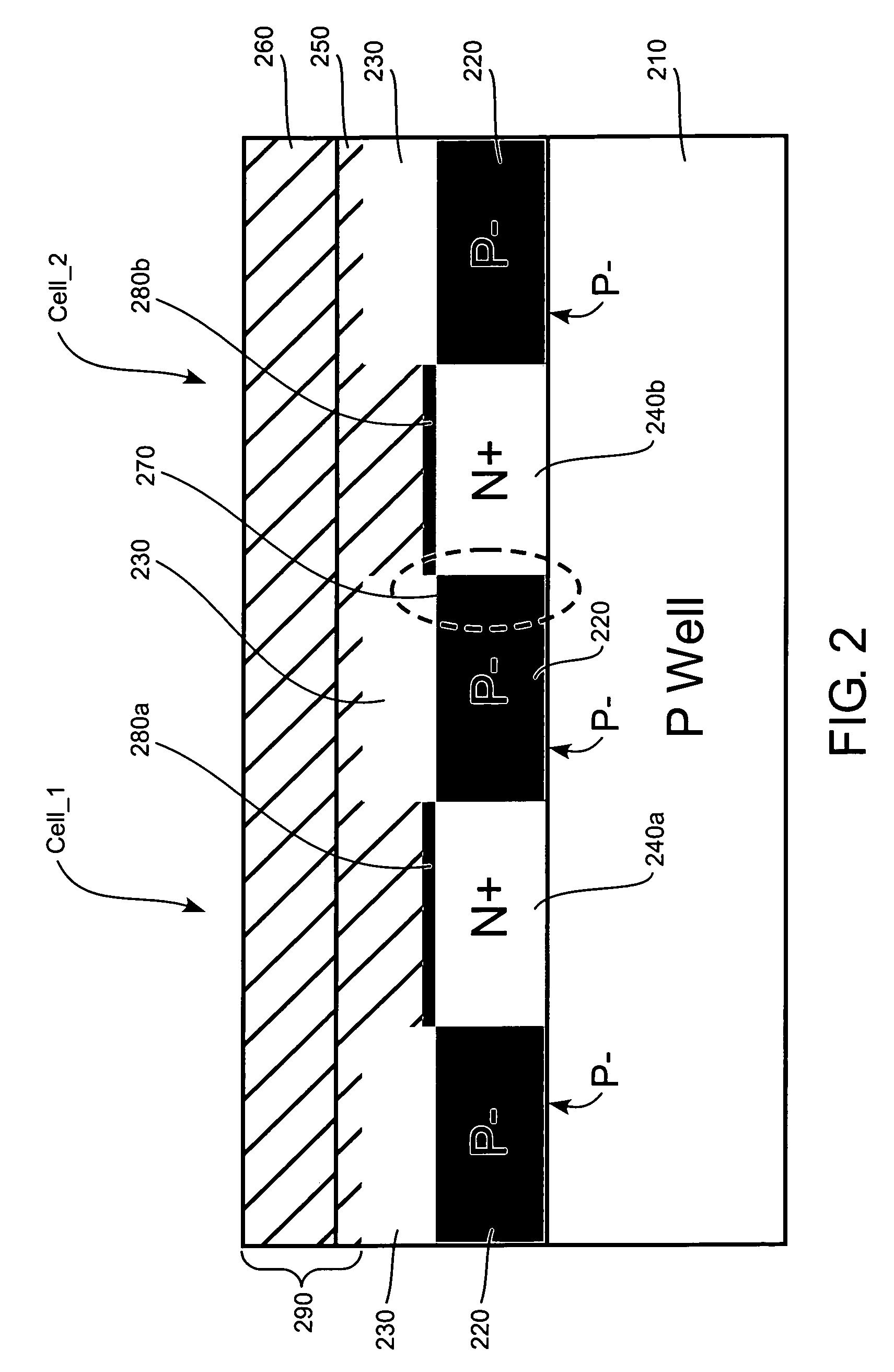
[0026]Referring initially to FIG. 1, a top view of an anti-fuse one-time-programmable (OTP) nonvolatile memory array 100 is shown in a...


PUM


Abstract

An anti-fuse one-time-programmable (OTP) nonvolatile memory cell has a P well substrate with two P− doped regions. Another N+ doped region, functioning as a bit line, is positioned adjacent and between the two P− doped regions on the substrate. An anti-fuse is defined over the N+ doped region. Two insulator regions are deposited over the two P− doped regions. An impurity doped polysilicon layer is defined over the two insulator regions and the anti-fuse. A polycide layer is defined over the impurity doped polysilicon layer. The polycide layer and the polysilicon layer function as a word line. A programmed region, i.e., a link, functioning as a diode, is formed on the anti-fuse after the anti-fuse OTP nonvolatile memory cell is programmed. The array structure of anti-fuse OTP nonvolatile memory cells and methods for programming, reading, and fabricating such a cell are also disclosed.

Description

BACKGROUND OF THE INVENTION[0001]1. Field of the Invention[0002]The present invention relates generally to a nonvolatile memory cell, and more particularly, to an anti-fuse one-time-programmable nonvolatile memory cell(s) and methods for fabricating, programming, and reading such a cell(s).[0003]2. Description of the Related Art[0004]With the rapid development of consumer electronic products, solid-state data storage has become increasingly important. The small size, simple structure, and low cost of the solid-state data storage are especially desired for portable consumer products. Solid-state data storage technologies like EPROM and EEPROM have been optimized for high-speed applications, resulting in complex and expensive processes. However, for many consumer applications, low cost is more important than speed.[0005]The prior art teaches diode programmable read only memories (DPROMs), however, the fabrication process of such DPROM cells is too complex due to the needs for deep tre...

Claims


Application Information

Patent Timeline
Patent Type & Authority Patents(United States)
IPC IPC(8): H01L29/00
CPCH01L23/5252H01L27/1021G11C17/00H01L2924/3011H01L2924/0002H01L2924/00
Inventor LUNG, HSIANG-LAN
Owner MACRONIX INT CO LTD
Why Eureka
Try Eureka