Power semiconductor device

a technology of semiconductor devices and super junctions, applied in semiconductor devices, semiconductor/solid-state device details, electrical apparatus, etc., can solve the problems of high processing difficulty, easy depletion of super junction structures at a lower voltage, and trade-off between device breakdown voltage and breakdown voltag

Inactive Publication Date: 2010-01-05
KK TOSHIBA
View PDF8 Cites 47 Cited by
  • Summary
  • Abstract
  • Description
  • Claims
  • Application Information

AI Technical Summary

Problems solved by technology

Thus there is a tradeoff between the device breakdown voltage and the ON resistance.
However, unfortunately, the decrease of the repetition period of the super junction structure will increase processing difficulty.
By burying the electrode in the n-pillar layer, the super junction structure is easily depleted at a lower voltage.
However, upon application of high voltage, electric field concentration occurs at the bottom of the trench because of the electrode buried in the trench.
When the electric field strength increases at the bottom of the trench and causes avalanche breakdown, holes generated by the breakdown are injected into the insulating film in the trench and degrade the insulation of the insulating film.
Thus local electric field concentration degrades the long-term reliability of the device.

Method used


Image

  • Power semiconductor device
  • Power semiconductor device
  • Power semiconductor device

Examples


first embodiment

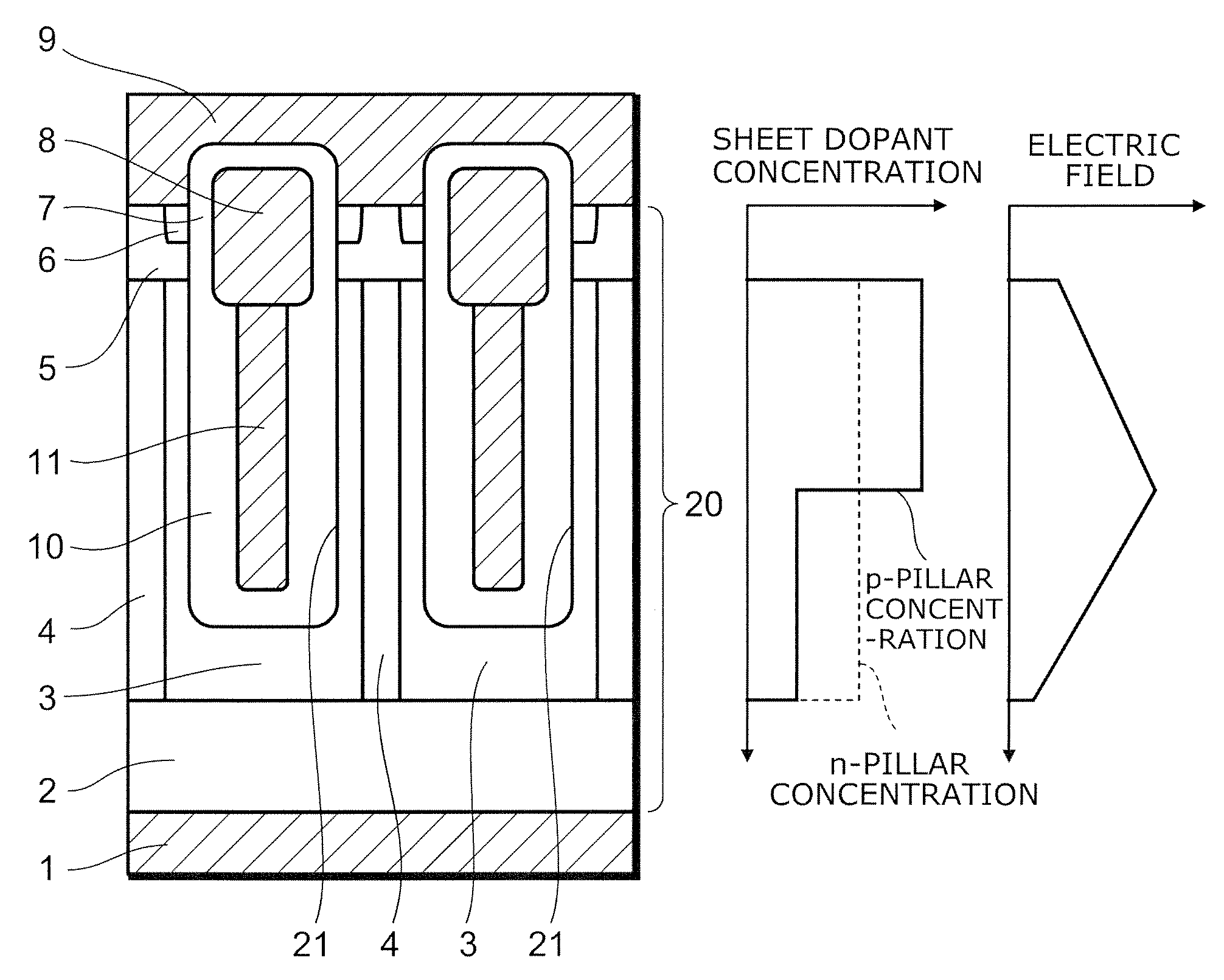
[0038]FIG. 1 shows a cross-sectional view schematically illustrating a power MOSFET according to a first embodiment of the invention, and schematic graphs illustrating sheet dopant concentration and electric field strength in its pillar layers in correlation with position along the depth direction.

[0039]It is noted that FIG. 1 shows only the cell section of the power MOSFET. The same also applies to FIGS. 2 to 17 described below. The term “sheet dopant concentration” in the pillar layer refers to a value given by the product of dopant concentration and pillar width at an arbitrary position along the depth direction of the pillar layer.

[0040]As shown in FIG. 1, the power MOSFET 101 according to this embodiment includes a semiconductor substrate 20, which is illustratively an n-type silicon substrate. An n+-drain layer 2 serving as a first semiconductor layer is formed in the lower portion of the semiconductor substrate 20. A drain electrode 1 serving as a first main electrode is prov...

second embodiment

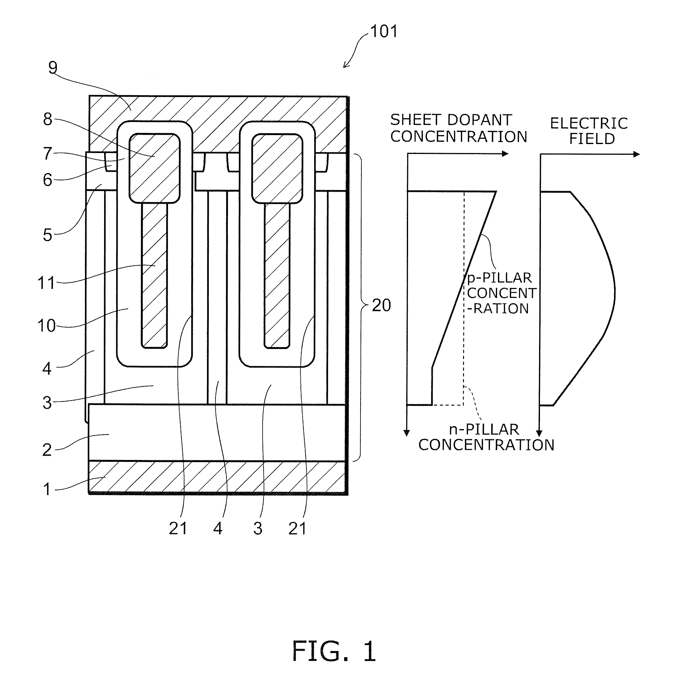
[0067]FIG. 6 shows a cross-sectional view schematically illustrating a power MOSFET according to a second embodiment of the invention, and schematic graphs illustrating sheet dopant concentration and electric field strength in its pillar layers in correlation with position along the depth direction.

[0068]In FIG. 6, the detailed description of the same elements as those in FIG. 1 is omitted, and only different elements are described here.

[0069]As shown in FIG. 6, in the power MOSFET 102 according to this embodiment, the trench 21 is formed so as to enter the boundary portion between the n-pillar layer 3 and the p-pillar layer 4. Thus only one of the n-pillar layer 3 and the p-pillar layer 4 exists in each portion of the drift layer between the trenches 21. As compared with the first embodiment described above, the trench 21 is shallower, formed only halfway through the drift layer. Furthermore, the p-pillar layer 4 is not in contact with the n+-drain layer 2, but the p-pillar layer 3...

third embodiment

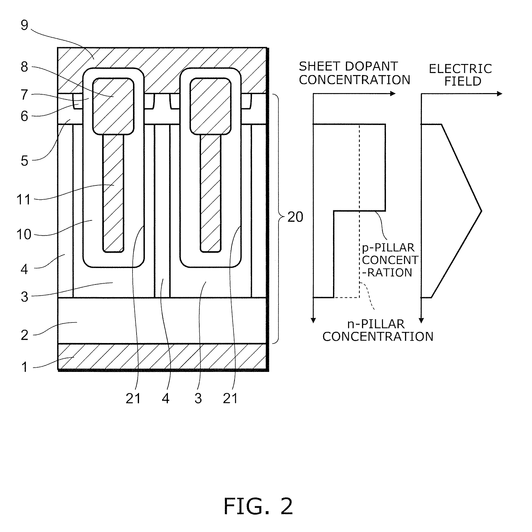
[0078]FIG. 8 shows a cross-sectional view schematically illustrating a power MOSFET according to a third embodiment of the invention, and schematic graphs illustrating sheet dopant concentration and electric field strength in its pillar layers in correlation with position along the depth direction.

[0079]In FIG. 8, the detailed description of the same elements as those in FIG. 1 is omitted, and only different elements are described here.

[0080]As shown in FIG. 8, in the power MOSFET 103 according to this embodiment, the width of the buried field plate electrode 11 varies along the depth direction in its lower portion, thinned downward. On the other hand, the width of the trench 21 is constant along the depth direction. Hence the thickness of the buried insulating film 10 varies along the depth direction, being constant and as thin as the gate insulating film 7 in the upper portion of the trench 21, but thickened downward in the lower portion thereof. The n-pillar concentration and the...


PUM


Abstract

A power semiconductor device includes a semiconductor substrate having a plurality of trenches formed in an upper surface thereof; a buried insulating film; a buried field plate electrode; a control electrode; a first main electrode provided on a lower side of the semiconductor substrate; and a second main electrode provided on an upper side of the semiconductor substrate. The semiconductor substrate includes: a first semiconductor; a second semiconductor layer of the first conductivity type and a third semiconductor layer of a second conductivity type; a fourth semiconductor layer; and a fifth semiconductor layer. The buried insulating film is thicker than a gate insulating film. At least one of the second semiconductor layer and the third semiconductor layer has a portion with its sheet dopant concentration varying along a depth direction of the semiconductor substrate.

Description

CROSS-REFERENCE TO RELATED APPLICATIONS[0001]This application is based upon and claims the benefit of priority from the prior Japanese Patent Application No. 2006-308406, filed on Nov. 14, 2006; the entire contents of which are incorporated herein by reference.BACKGROUND OF THE INVENTION[0002]1. Field of the Invention[0003]This invention relates to a power semiconductor device, and more particularly to a power semiconductor device having a super junction structure.[0004]2. Background Art[0005]The ON resistance of a power semiconductor device such as a vertical power MOSFET (metal oxide semiconductor field effect transistor) greatly depends on the electric resistance of its conduction layer (drift layer). The dopant concentration that determines the electric resistance of the drift layer cannot exceed a maximum limit, which depends on the breakdown voltage of a pn junction between the base layer and the drift layer. Thus there is a tradeoff between the device breakdown voltage and th...

Claims


Application Information

Patent Timeline
Patent Type & Authority Patents(United States)
IPC IPC(8): H01L27/088
CPCH01L29/0634H01L29/407H01L29/42368H01L29/7811H01L29/7812H01L29/0615H01L29/0619H01L29/0623H01L29/063H01L29/0638H01L29/0878H01L29/1095H01L29/402H01L29/41741
Inventor SAITO, WATARU
Owner KK TOSHIBA
Why Eureka
Try Eureka