

High speed current mode write driver
a current mode and write driver technology, applied in the field of integrated circuits, can solve the problems of sluggish saturated h-bridge transistors, difficult to prevent saturation and cutoff of h-bridges, dead bands, etc., and achieve the effect of low power operation and high switching speed
Active Publication Date: 2010-01-05
TEXAS INSTR INC
View PDF6 Cites 9 Cited by
- Summary
- Abstract
- Description
- Claims
- Application Information
AI Technical Summary
Benefits of technology
The invention provides integrated circuits with current mode write drivers that operate without the need for voltage conversions, which eliminates dead bands and saturated transistors. These write drivers directly convert received voltages into currents for delivery to the load, resulting in faster switching and lower power operation. The invention also includes a switching control circuit with a DC current control circuit and a boost current control circuit that can convert ECL differential voltage signals into DC and boost output currents for delivery to the load through a current mirror. The technical effects of the invention include improved performance and efficiency of current mode write drivers.
Problems solved by technology
The technical problem addressed in this patent text is the need for new write driver designs that provide higher switching speed, while at the same time providing low power operation to prevent saturation and cutoff of H-bridge transistors and to reduce dead bands and sluggishness in the recovery process.
Method used
View moreImage
Smart ImageViewing Examples

Examples
examples
[0042]The following non-limiting Examples serve to illustrate selected embodiments of the invention. It will be appreciated that variations in proportions and alternatives in elements of the components shown will be apparent to those skilled in the art and are within the scope of embodiments of the present invention.
[0043]Simulations were preformed to generate eye patterns and minimum duration data for the write driver 200 shown in FIG. 2A as compared to a conventional current mode write driver that as described above performs input voltage to current to voltage to write current. Inputs were 300 mV ECL signals. The data rate for write driver 200 was found to be double the data rate for this conventional write driver.
Login to View More PUM
 Abstract
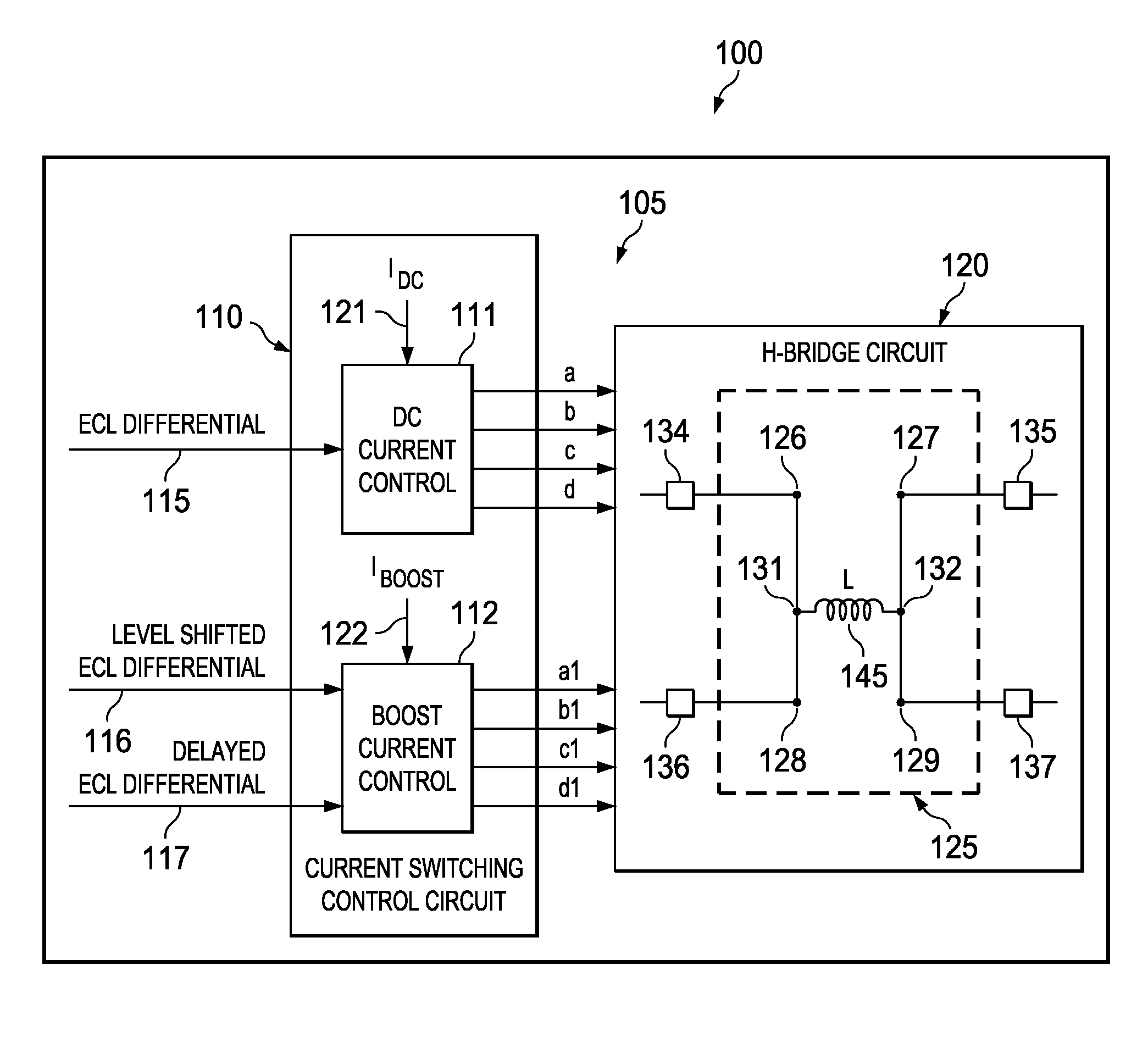
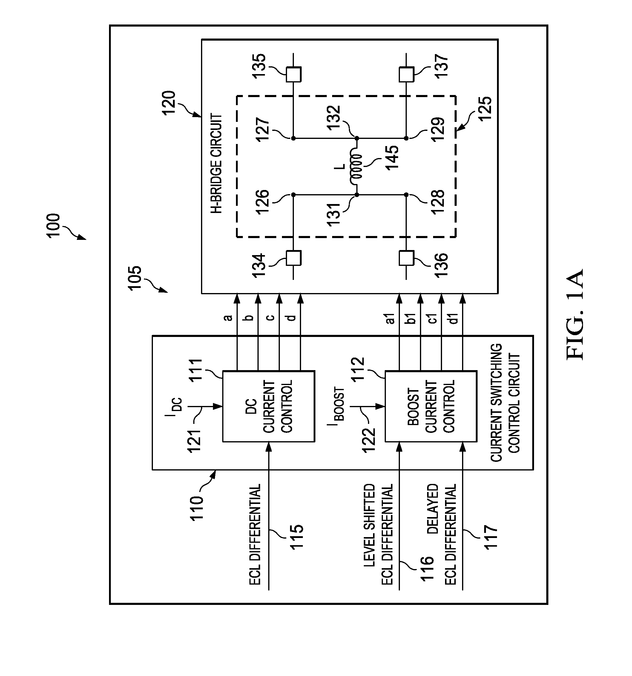
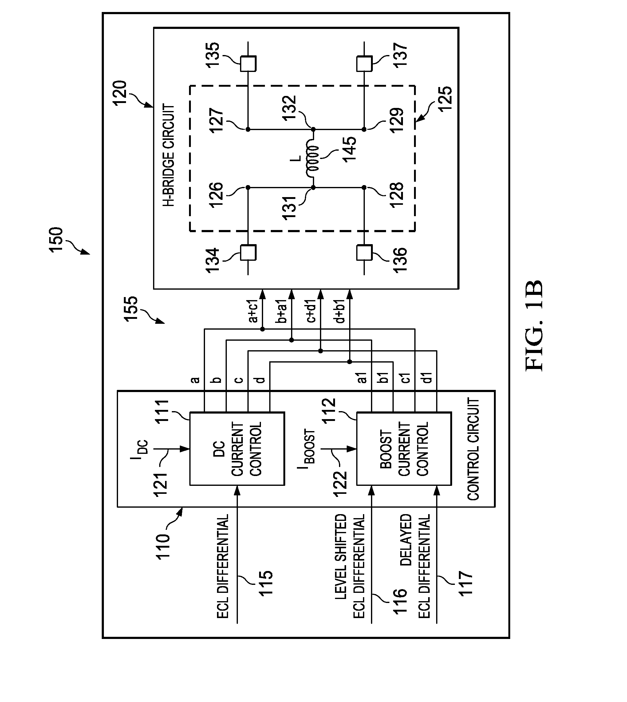
An integrated circuit (100) includes a current mode write driver (105). The write driver (105) includes a switching control circuit (110) including (i) a DC current control circuit (111) operable to directly convert a received ECL differential signal into first, second, third and fourth DC output currents (a, b, c, and d) and (ii) a boost current control circuit (112) operable to directly convert a received level shifted version of the ECL differential voltage signal and a delayed version of the ECL differential voltage signal into first, second, third and fourth boost output currents (a1, b1, c1, and d1). An H-bridge circuit (120) includes an output stage (125) including first and second current sourcing control nodes (126, 127) and first and second current sinking control nodes (128, 129). A first output node (131) is between the first sourcing and first sinking nodes (126, 128) and second output node between the second sourcing and the second sinking nodes (127, 129). A first, second, third and fourth current mirror including input is coupled to sourcing or sinking control nodes (126, 127, 128, and 129) and are each operable to receive one of the DC output currents and one of the boost output currents for switchably delivering current diagonally through a load (145) connected between the output nodes (131, 132).
Description
Login to View More Claims
Login to View More Application Information
Patent Timeline
 OwnerTEXAS INSTR INC