Fabrication of low dielectric constant insulating film

a technology of insulating film and dielectric constant, which is applied in the direction of crystal growth process, polycrystalline material growth, instruments, etc., can solve the problems of deteriorating adhesion of film, reducing film thickness, and preventing the performance gain of semiconductor integrated circuits. achieve the effect of improving adhesion of film without reducing film thickness

Inactive Publication Date: 2010-01-12
TOKYO ELECTRON LTD
View PDF22 Cites 0 Cited by
  • Summary
  • Abstract
  • Description
  • Claims
  • Application Information

AI Technical Summary

Benefits of technology

[0006]The main object of the present invention is to provide a method of lowering the dielectric constant of an insulating film without reducing the film-thickness, or of lowering the dielectric constant of an insulating film while improving the adhesion of the film by maintaining the film-hardness to the extent that the pattern thereof as formed can be maintained.
[0010]The present invention provides a method of forming a low-k insulating film, which includes the steps of: placing a substrate, on which an insulating film containing Si, O and CH is deposited by a chemical vapor deposition process, in a reaction vessel; supplying a process gas containing hydrogen atoms into the reaction vessel and supplying a microwave into the reaction vessel, thereby generating a plasma containing hydrogen radicals; and modifying a structure of the insulating film deposited on the substrate by means of the hydrogen radical contained in the plasma, thereby lowering a dielectric constant of the insulating film.
[0019]The present invention further provides a method of forming a low-k insulating film, which includes the steps of: placing a substrate, on which an insulating film containing Si, O and CH is deposited by a chemical vapor deposition process under a process temperature of 100° C. or below, in a reaction vessel; supplying a process gas containing hydrogen atoms into the reaction vessel and supplying an electromagnetic wave into the reaction vessel, thereby generating a plasma containing hydrogen radicals; and modifying a structure of the insulating film deposited on the substrate by means of the hydrogen radicals contained in the plasma, thereby lowering a dielectric constant of the insulating film.
[0020]The present invention further provides a method of forming a low-k insulating film, which includes the steps of: placing a substrate, on which an insulating film containing Si, O and CH is deposited by a chemical vapor deposition process, in a reaction vessel; supplying hydrogen gas and argon gas only into the reaction vessel supplying an electromagnetic wave into the reaction vessel, thereby generating a plasma containing hydrogen radicals; and modifying a structure of the insulating film deposited on the substrate by means of the hydrogen radicals contained in the plasma, thereby lowering a dielectric constant of the insulating film.

Problems solved by technology

With high integration of semiconductor integrated circuits, increase of interconnect-delay due to increase of interconnect-capacitance, namely, parasitic capacitance between metallic wires, prevents the performance gain of semiconductor integrated circuits.
However, the above method does not modify the structure of the interlayer insulating film itself, but just vaporizes almost the organic components in the organic-inorganic composite film to make Si—H bonds by a plasma treatment or a heat treatment, thereby to form a number of fine pores at sites from which organic components have been vaporized.
The film after processed becomes porous, and thus the film shrinks, resulting in reduction of the film thickness and deterioration in adhesion of the film due to increase of the film hardness.

Method used


Image

  • Fabrication of low dielectric constant insulating film
  • Fabrication of low dielectric constant insulating film
  • Fabrication of low dielectric constant insulating film

Examples


Embodiment Construction

[0048]The embodiments of the present invention will be described below.

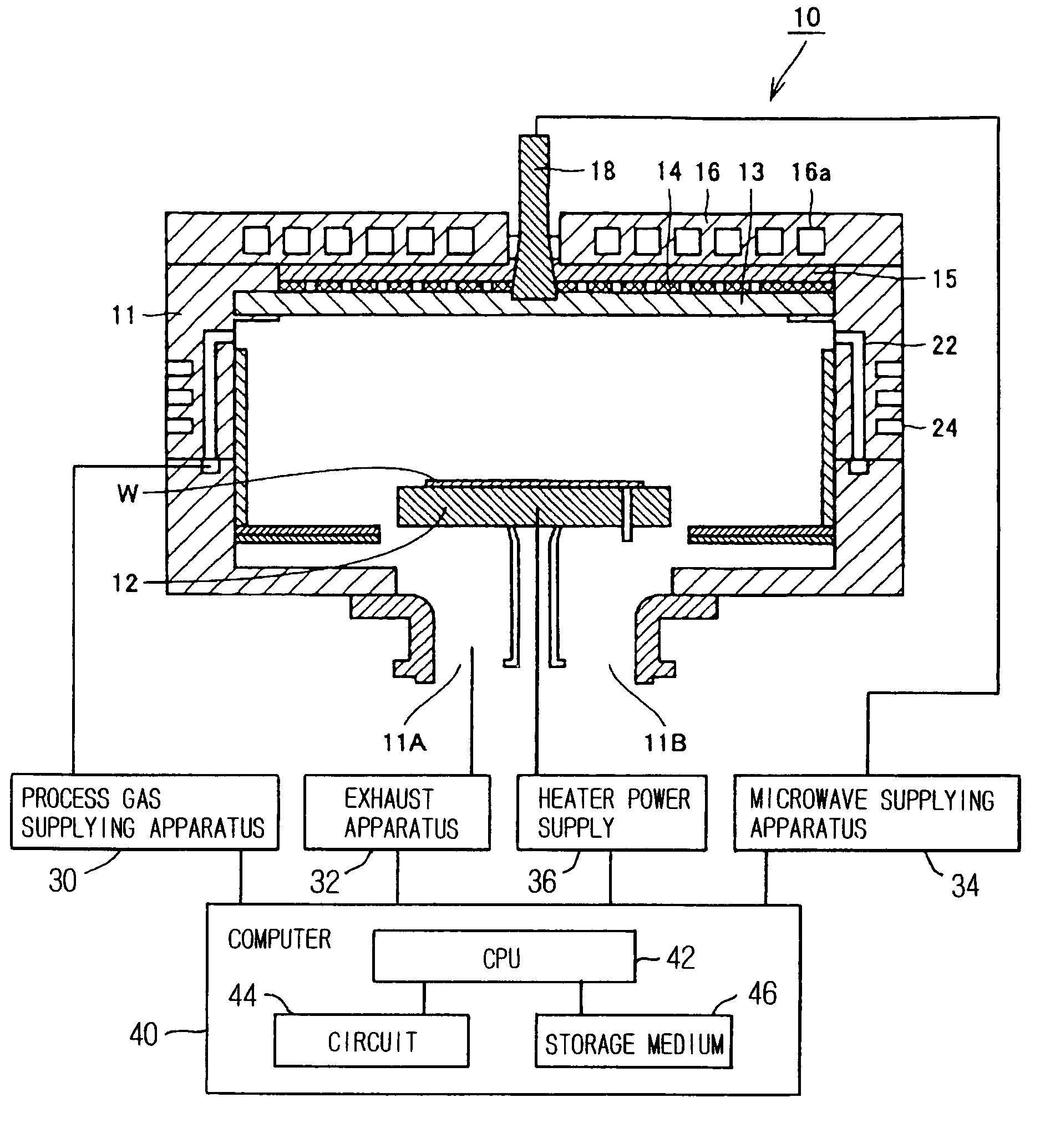
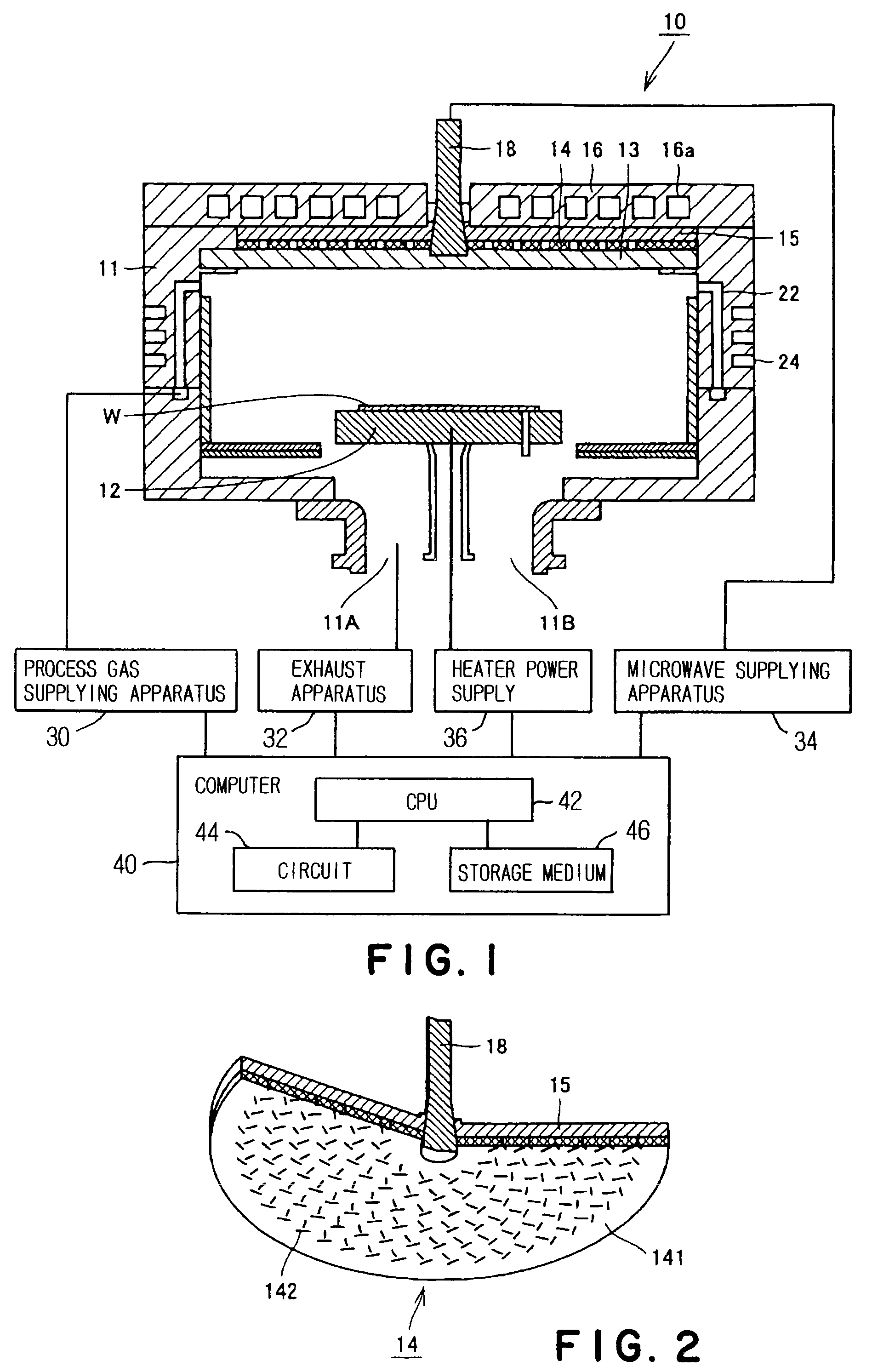
[0049]FIG. 1 is a cross-sectional view of a plasma substrate processing system used for forming an insulating film according to the present invention, and FIG. 2 is a partially-broken perspective view of a slot plate (antenna) shown in FIG. 1.

[0050]The plasma substrate processing system 10 includes a processing vessel 11 provided therein with a pedestal 12 for holding a silicon wafer W which is a substrate to be processed. Gases in the processing vessel 11 are discharged therefrom through exhaust ports 11A and 11B by a not shown exhaust pump. The pedestal 12 has a heating function for heating the silicon wafer W.

[0051]The upper portion of the processing vessel 11 is provided with an opening so as to oppose the silicon wafer W on the pedestal 12. The opening is closed by a dielectric plate 13 of quartz or aluminum oxide. A slot plate 14 shown in FIG. 2, which functions as a planer antenna, is arranged above (outsi...


PUM

PropertyMeasurementUnit
temperatureaaaaaaaaaa
dielectric constantaaaaaaaaaa
pressureaaaaaaaaaa

Abstract

The present invention relates to a method of lowering dielectric constant of an insulating film including Si, O and CH formed by a chemical vapor deposition process. A process gas containing hydrogen atoms is supplied into a reaction vessel. A microwave is introduced into the reaction vessel to supply a uniform electromagnetic wave, thereby a plasma containing a hydrogen radical is generated in the reaction vessel. The structure of the insulating film is modified by the hydrogen radical contained in the plasma irradiated to the insulating film, lowering the dielectric constant of the film. The microwave is supplied into the reaction vessel through a radial-slot antenna.

Description

TECHNICAL FIELD[0001]The present invention relates to a low dielectric constant (low-k) insulating film, and more specifically to a technique for lowering the dielectric constant of an insulating film by processing it with plasma.BACKGROUND ART[0002]With high integration of semiconductor integrated circuits, increase of interconnect-delay due to increase of interconnect-capacitance, namely, parasitic capacitance between metallic wires, prevents the performance gain of semiconductor integrated circuits. The interconnect-delay is proportional to the product of the resistance of metallic wires and the interconnect-capacitance. In order to reduce the interconnect-delay by reducing the resistance of metallic wires, copper (Cu) having a high conductivity is recently used in place of previously-used aluminum (Al).[0003]On the other hand, the dielectric constant (k) of an interlayer insulating film formed between the metallic wires may be lowered to decrease the interconnect-capacitance. In...

Claims


Application Information

Patent Timeline
Patent Type & Authority Patents(United States)
IPC IPC(8): C23C16/00C04B41/00C30B17/00C30B28/12C23C16/40H01L21/3105H01L21/312H01L21/316
CPCC23C16/401H01J37/32192H01J37/32935H01L21/02126H01L21/02203H01L21/02211H01L21/02274H01L21/0234H01L21/3003H01L21/31058H01L21/3121H01L21/31633H01L21/31695
Inventor SASAKI, MASARUHOSHINO, SATOHIKOIDE, SHINJIKASHIWAGI, YUSAKU
Owner TOKYO ELECTRON LTD
Why Eureka
Try Eureka