
Method of fabricating a semiconductor device including separately forming a second semiconductor film containing an impurity element over the first semiconductor region

a semiconductor and film technology, applied in the direction of semiconductor devices, basic electric elements, electrical appliances, etc., can solve the problems of serious image quality degradation, uneven illumination, and limitation of tft using amorphous semiconductor films, and achieve low wiring resistance, less impurity metal elements, and improved image quality

Inactive Publication Date: 2010-01-19
SEMICON ENERGY LAB CO LTD
View PDF8 Cites 31 Cited by
  • Summary
  • Abstract
  • Description
  • Claims
  • Application Information

AI Technical Summary

Benefits of technology

The invention provides a method of fabricating a semiconductor device with an inversely staggered TFT that can operate at high speeds and has few variations in threshold. The method also reduces the cost of materials and improves the yield of the semiconductor device. The invention also provides a display device with high image contrast and excellent switching properties. The method includes forming a gate electrode, adding a catalytic element, heating the semiconductor film, adding a layer containing a donor element or a rare gas element, adding a layer containing a donor element and a rare gas element, forming a semiconductor region, adding a second semiconductor region containing an impurity element, forming a first conductive layer, and forming a second conductive layer.

Problems solved by technology

Therefore, in the display device using such a TFT formed of an amorphous semiconductor film for switching of the pixel, luminance unevenness occurs.
Such a phenomenon is recognized more easily in a large-screen TV having a diagonal size of 30 inches or larger (typically, 40 inches or larger), which thus poses a serious problem on the degradation in image quality.
However, the TFT using an amorphous semiconductor film has a limitation.
For example, it is difficult to realize a liquid crystal display device of the OCB mode.
However, most of the film deposited over the whole surface of the substrate by the CVD method, the PVD method or the like and the material of the resist or the like are wasted as well as the number of steps for forming the wiring or the semiconductor region is increased, which results in the lower throughput.

Method used


Image

  • Method of fabricating a semiconductor device including separately forming a second semiconductor film containing an impurity element over the first semiconductor region
  • Method of fabricating a semiconductor device including separately forming a second semiconductor film containing an impurity element over the first semiconductor region
  • Method of fabricating a semiconductor device including separately forming a second semiconductor film containing an impurity element over the first semiconductor region

Examples


embodiment mode 1

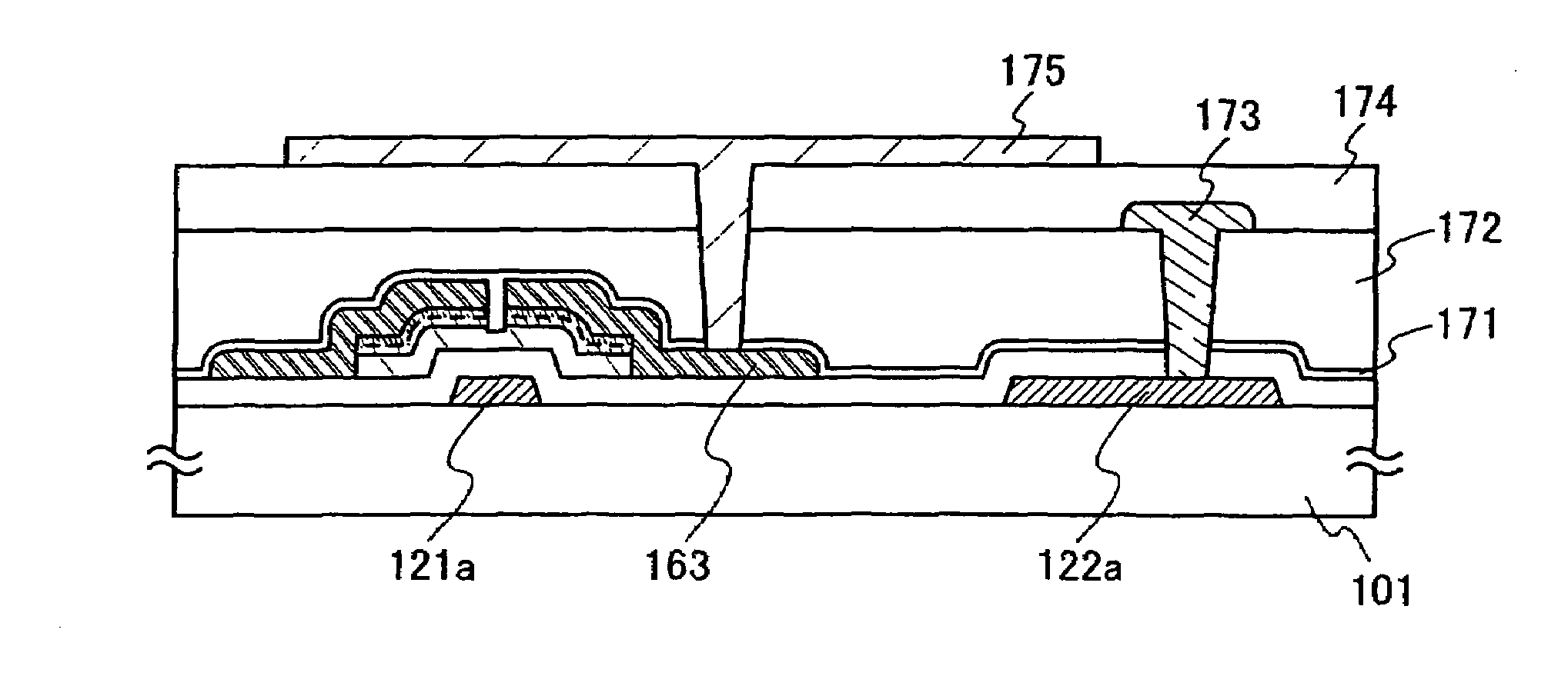
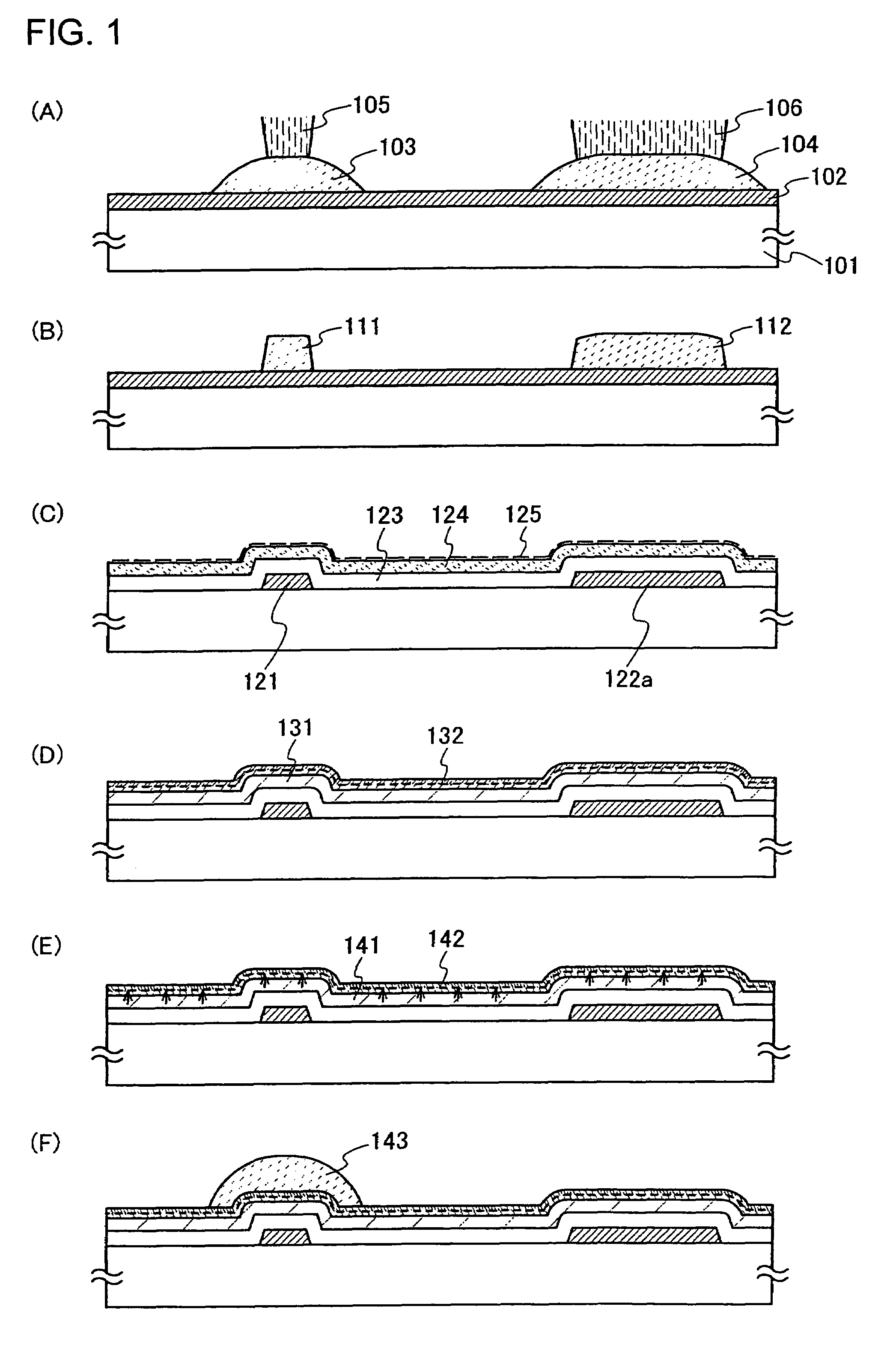
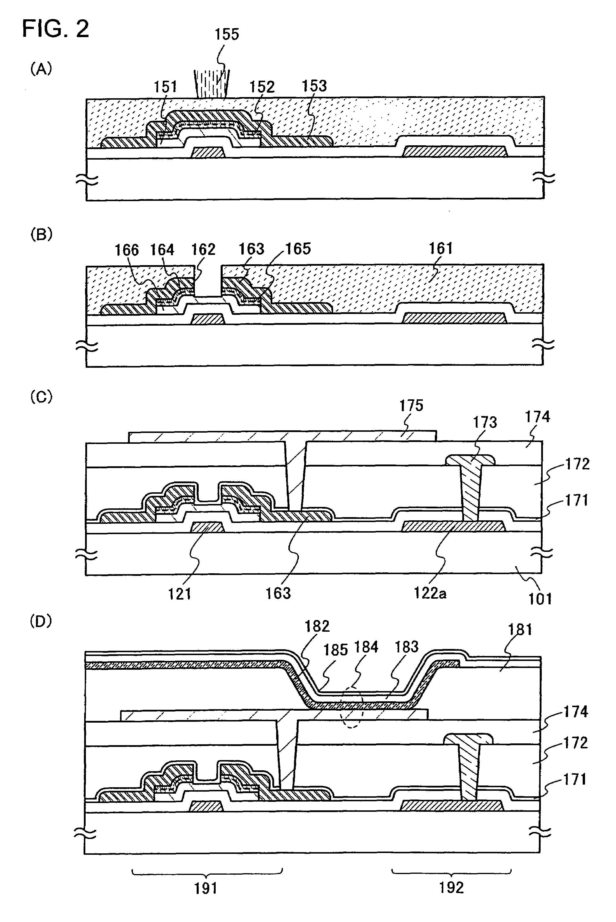
[0048]In this embodiment mode, description is made with reference to FIGS. 1 to 3, 26 and 51 on fabrication steps of an active matrix substrate in which an inversely staggered TFT having a crystalline semiconductor film is used as an element for driving a light-emitting element. In this embodiment mode, a switching TFT and a driving TFT are shown as typical examples of an element for driving a light-emitting element. FIG. 3 shows cross-sectional views and a top view of the switching TFT and the driving TFT. FIGS. 1 and FIGS. 2 show cross-sectional views illustrating a connection portion of a gate electrode and a gate wiring of a switching TFT, a driving TFT and a light-emitting element.

[0049]As shown in FIG. 1(A) a first conductive layer 102 is formed over a substrate 101, and photosensitive materials 103 and 104 are applied onto the first conductive layer, and then dried and baked. Then, the photosensitive materials 103 and 104 are irradiated with laser light (hereinafter also refe...

embodiment mode 2

[0126]In this embodiment mode, description is made with reference to FIG. 3 on a stacked-layer structure of a power source line, a source wiring, a source electrode or drain electrode, a gate wiring, and a pixel electrode of the active matrix substrate shown in Embodiment Mode 1. An embodiment mode below shows vertical cross-sectional views and a top view corresponding to FIG. 2(C) before the formation of the light-emitting element.

[0127]FIG. 3(A) is a view showing a stacked-layer structure of the driving TFT 191 and the fifth conductive layer functioning as a gate wiring of the switching TFT 192, which corresponds to the cross-sectional structure along A-B of FIG. 3(C).

[0128]FIG. 3(B) is a view showing a connection structure of the switching TFT 192 and the driving TFT 191, which corresponds to the cross-sectional structure along C-D of FIG. 3(C).

[0129]Hereinafter, the fourth conductive layer functioning as a power source line and a capacitor wiring is denoted by a power source lin...

embodiment mode 4

[0145]In this embodiment mode, description is made with reference to FIG. 5 on an active matrix substrate having a different structure of a gate wiring from Embodiment Mode 2.

[0146]FIG. 5(A) is a view showing a stacked-layer structure of the driving TFT 191 and the gate wiring of the switching TFT 192, which corresponds to the cross-sectional structure along A-B of FIG. 5(C).

[0147]FIG. 5(B) is a view showing a connection structure of the switching TFT 192 and the driving TFT 191, which corresponds to the cross-sectional structure along C-D of FIG. 5(C).

[0148]In this embodiment mode, the structures of the driving TFT 191, the switching TFT 192 and the capacitor 193 are similar to those in Embodiment Mode 2. Note that as shown in FIG. 5(C), gate wirings 1123a and 1123b are formed in each pixel, and connected to gate electrodes 122a and 122b which are provided in adjacent pixels. Therefore, the material of the gate wirings 1123a and 1123b is not specifically required to be a low-resist...


PUM

PropertyMeasurementUnit
sizeaaaaaaaaaa
sizeaaaaaaaaaa
sizeaaaaaaaaaa

Abstract

The invention provides a method of fabricating a semiconductor device having an inversely staggered TFT capable of high-speed operation, which has few variations of the threshold. In addition, the invention provides a method of fabricating a semiconductor device with high throughput where the cost reduction is achieved with few materials.According to the invention, a semiconductor device is fabricated by forming an inversely staggered TFT which is obtained by forming a gate electrode using a highly heat-resistant material, depositing an amorphous semiconductor film, adding a catalytic element into the amorphous semiconductor film and heating the amorphous semiconductor film to form a crystalline semiconductor film, forming a layer containing a donor element or a rare gas element over the crystalline semiconductor film and heating the layer to remove the catalytic element from the crystalline semiconductor film, forming a semiconductor region by utilizing a part of the crystalline semiconductor film, forming a source electrode and a drain electrode to be electrically connected to the semiconductor region, and forming a gate wiring to be connected to the gate electrode.

Description

INDUSTRIAL FIELD OF THE INVENTION[0001]The present invention relates to a method of fabricating a semiconductor device having an inversely staggered thin film transistor which is formed of a crystalline semiconductor film.PRIOR ART[0002]In recent years, a flat panel display (FPD) typified by a liquid crystal display (LCD) or an EL display is attracting attention as an alternative display device for a conventional CRT In particular, development of a large-screen liquid crystal television mounted with a large liquid crystal display panel which is driven by an active matrix method is the primary task for liquid crystal panel manufacturers. In recent years, a large-screen EL television has also been developed following the liquid crystal television.[0003]In a conventional liquid crystal display device or display device having light-emitting elements, a thin film transistor (hereinafter referred to as a TFT) which uses amorphous silicon is used as a semiconductor element for driving each...

Claims


Application Information

Patent Timeline
Patent Type & Authority Patents(United States)
IPC IPC(8): H01L21/00
CPCH01L27/1214H01L27/124H01L27/1251H01L27/1277H01L27/1288
Inventor YAMAZAKI, SHUNPEIMAEKAWA, SHINJIHONDA, TATSUYASHOJI, HIRONOBUNAKAMURA, OSAMUSUZUKI, YUKIEKAWAMATA, IKUKO
Owner SEMICON ENERGY LAB CO LTD
Features
  • Generate Ideas
  • Intellectual Property
  • Life Sciences
  • Materials
  • Tech Scout
  • Unparalleled Data Quality
  • Higher Quality Content
  • 60% Fewer Hallucinations
Learn More