Packaging substrate having heat-dissipating structure

a technology of packaging substrate and heat dissipation structure, which is applied in the direction of semiconductor devices, semiconductor/solid-state device details, electrical devices, etc., can solve the problems of shortened service life of semiconductor chips, deterioration of performance, and hardly conducive to miniaturization and improvement in performance in the early stages of the art, so as to enhance heat dissipation, enhance heat dissipation, and reduce the effect of heat loss

Active Publication Date: 2010-02-02
PHOENIX PRECISION TECH CORP
View PDF2 Cites 37 Cited by
  • Summary
  • Abstract
  • Description
  • Claims
  • Application Information

AI Technical Summary

Benefits of technology

[0010]In view of the aforesaid drawbacks of the prior art, it is the primary objective of the present invention to provide a packaging substrate having a heat-dissipating structure so as to efficiently dissipate heat generated by a semiconductor chip in operation.
[0011]Another objective of the present invention is to provide a packaging substrate having a heat-dissipating structure so as to evade increasing thickness and weight of package structures and incurring costs.
[0012]Yet another objective of the present invention is to provide a packaging substrate having a heat-dissipating structure so as to evade increasing the size of the packaging substrate but enhance the electrical performance of the packaging substrate.
[0013]A further objective of the present invention is to provide a packaging substrate having a heat-dissipating structure so as to protect the packaging substrate against warpage by forming a wiring layer on both sides of the packaging substrate.
[0016]Optionally, an adhesive fills the gap between the semiconductor chip and the first cavity, thereby fixing the semiconductor chip in the first cavity. Also, the adhesive fills the gap between the semiconductor chip and the second cavity, thereby fixing the semiconductor chip in the second cavity. Alternatively, the dielectric layer fills the gap between the semiconductor chip and the first cavity, thereby fixing the semiconductor chip in the first cavity, also the dielectric layer fills the gap between the semiconductor chip and the second cavity, thereby fixing the semiconductor chip in the second cavity.
[0019]The present invention provides a packaging substrate having a heat-dissipating structure. The packaging substrate comprises a plurality of semiconductor chips mounted on the first metal layer and the second metal layer exposed from the first cavity and the second cavity in a core layer. Heat generated by the semiconductor chips in operation is taken by the first metal layer and the second metal layer and then transferred to a heat-conduction component via a heat-dissipating through hole, so as to enhance heat dissipation. The first metal layer and the second metal layer disposed on the core layer and the heat-dissipating through hole penetrating the core layer and the build-up circuit structures not only enhance heat dissipation but also eliminate the drawbacks of the prior art, namely a plethora of components, excessive thickness, overweight, and high costs. The packaging substrate of the present invention features enhanced electrical performance and minimal thickness, and is free of warpage by forming a wiring layer on both sides of the packaging substrate.

Problems solved by technology

The prior art achieves a high pin number and yet is flawed by a resultant intricate layout on an unfavorably thick package structure due to limitation of semiconductor chips in surface area and size.
Hence, the prior art is hardly conducive to miniaturization and improvement in performance as far as semiconductor chip package structures are concerned.
An increasingly great amount of heat is generated by semiconductor chips in operation; procrastinated or inefficient dissipation of heat generated by the semiconductor chips in operation result in deteriorated performance and shortened service life of the semiconductor chips.
Although the aforesaid drawback of the prior art can be overcome with a solution, namely using a package structure which comprises a semiconductor chip-embedded substrate, the solution brings more problems.
Given a significant difference between the heat-dissipating board 12 and the dielectric layer 14 in coefficient of thermal expansion (CTE), variable thermal stress exhibited by individual components, together with unilateral build-up, is likely to cause warpage to the package structure.
Uncontrolled warpage may delaminate a package structure or crack a long-compressed semiconductor chip.
However, a thick heat-dissipating board accompanies a thick bulky package structure and incurs process costs.
Accordingly, an issue that prevails in the electronic industry and calls for immediate solution involves providing a packaging substrate structure for elimination of the drawbacks of the prior art, namely warpage, increased thickness and weight, and high costs.

Method used


Image

  • Packaging substrate having heat-dissipating structure
  • Packaging substrate having heat-dissipating structure
  • Packaging substrate having heat-dissipating structure

Examples


first embodiment

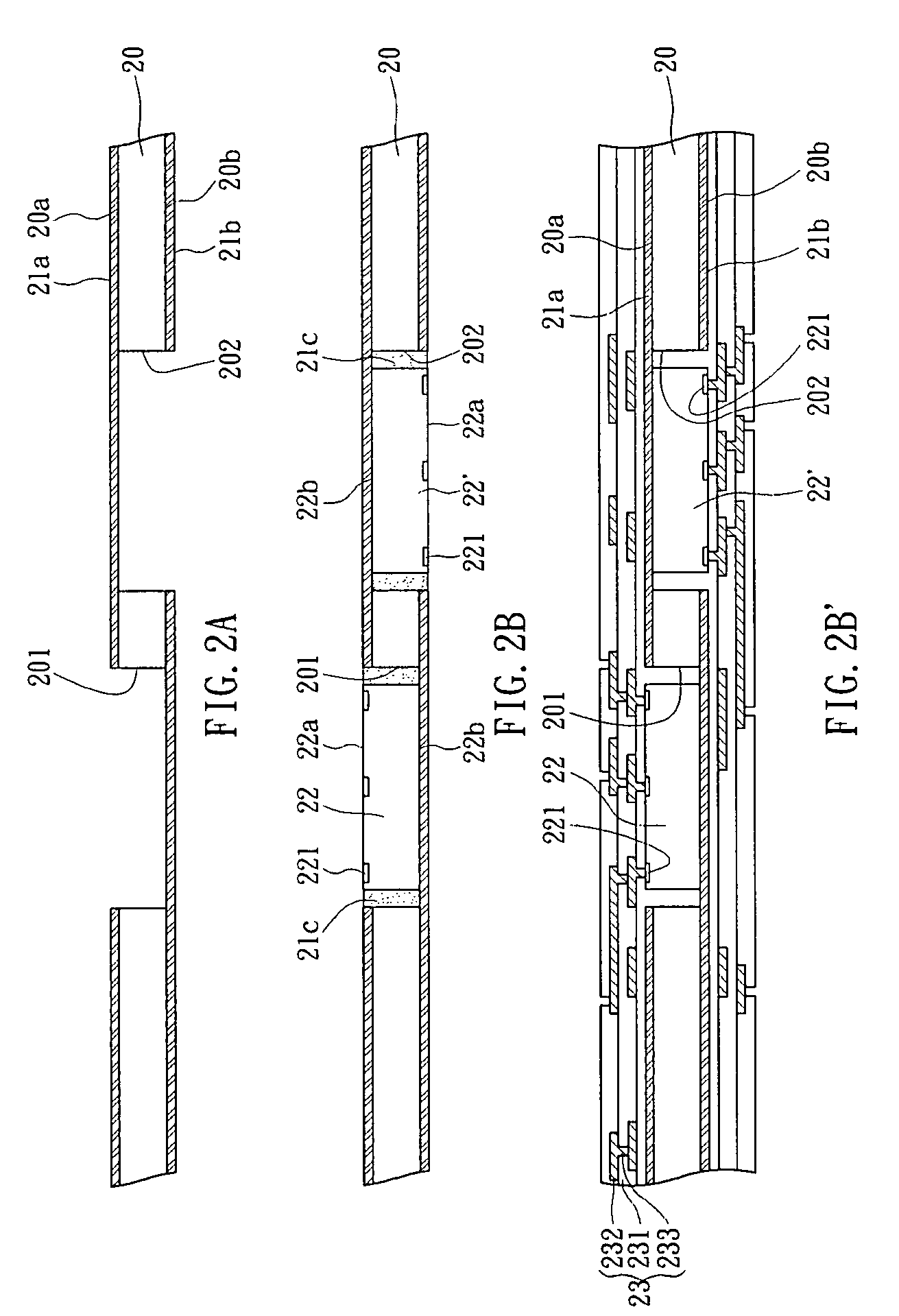
[0026]FIGS. 2A to 2F are cross-sectional views showing a first embodiment of a method for fabricating a packaging substrate having a heat-dissipating structure according to the present invention.

[0027]Referring to FIG. 2A, a core layer 20 such as a copper claded laminate (CCL) is provided. The copper claded laminate essentially comprise a composite board composed of an insulating layer sandwiched in between two copper foils. The core layer 20 has a first surface 20a and an opposite second surface 20b. The first surface 20a has a first metal layer 21a. The second surface 20b has a second metal layer 21b. A first cavity 201 is formed to penetrate the core layer 20 and the first metal layer 21a, thereby exposing the second metal layer 21b. A second cavity 202 is formed to penetrate the core layer 20 and the second metal layer 21b, thereby exposing the first metal layer 21a.

[0028]Referring to FIGS. 2B and 2B′, semiconductor chips 22, 22′ are received in the first cavity 201 and the sec...

second embodiment

[0036]FIGS. 3A to 3C are schematic views showing a second embodiment of a method for fabricating a packaging substrate having a heat-dissipating structure according to the present invention. The second embodiment differs from the first embodiment in that, in the second embodiment, conductive terminals (golden fingers) configured for use with expansion cards and expansion slots function as the conductive pads.

[0037]Referring to FIG. 3A, the structure shown in FIG. 2E is provided, wherein the outmost wiring layer 232′ of the build-up circuit structure 23 has a plurality of conductive pads functioning as conductive terminals (golden fingers) 234′.

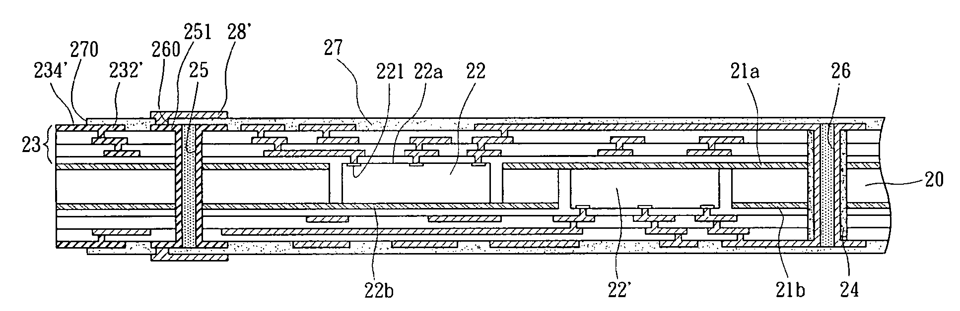
[0038]Referring to FIG. 3B, an insulating protective layer 27 is formed on the surface of the build-up circuit structures 23, and a plurality of openings 270 are formed in the insulating protective layer 27, thereby exposing the conductive terminals 234′ and the contact pad 251.

[0039]Referring to FIG. 3C, a heat-conduction component, such as a...


PUM

PropertyMeasurementUnit
heat-aaaaaaaaaa
conductiveaaaaaaaaaa
heat-dissipatingaaaaaaaaaa

Abstract

Provided is a packaging substrate with a heat-dissipating structure, including a core layer with a first surface and an opposite second surface having a first metal layer and a second metal layer respectively. Portions of the first metal layer are exposed from a second cavity penetrating the core layer and second metal layer. Portions of the second metal layer are exposed from a first cavity penetrating the core layer and first metal layer. Semiconductor chips each having an active surface with electrode pads thereon and an opposite inactive surface are received in the first and second cavities and attached to the second metal layer and the first metal layer respectively. Conductive vias disposed in build-up circuit structures electrically connect to the electrode pads of the semiconductor chips. A heat-dissipating through hole penetrating the core layer and build-up circuit structures connects the metal layers and contact pads.

Description

BACKGROUND OF THE INVENTION[0001]1. Field of the Invention[0002]The present invention relates to packaging substrate structures, and more particularly, to a packaging substrate having a heat-dissipating structure.[0003]2. Description of the Prior Art[0004]Owing to development of semiconductor packaging technology, semiconductor packages nowadays come in a variety of forms. Known methods for packaging semiconductor devices involve mounting an integrated circuit-laden semiconductor chip on a packaging substrate or a lead frame, electrically connecting the semiconductor chip to the packaging substrate or the lead frame, and encapsulating the packaging substrate with encapsulant. Ball Grid Array (BGA), which represents an advanced semiconductor packaging technology, is characterized by mounting a semiconductor chip on a packaging substrate and implanting a plurality of solder balls aligned in an array on the back of the packaging substrate, thereby increasing I / O connections provided on...

Claims


Application Information

Patent Timeline
Patent Type & Authority Patents(United States)
IPC IPC(8): H01L23/02
CPCH01L23/3677H01L24/24H01L24/82H01L25/0655H01L23/5389H01L2224/73267H01L2224/24227H01L2924/01029H01L2924/01082H01L2924/14H01L2924/15153H01L2924/15165H01L2924/1517H01L2924/01033H01L2224/04105H01L2224/12105H01L2224/32245H01L2924/351H01L2924/00
Inventor WONG, LIN-YINYEH, MAO-HUA
Owner PHOENIX PRECISION TECH CORP
Why Eureka
Try Eureka