Superhard cutters and associated methods

a cutter and superhard technology, applied in grinding drives, grinding drives, abrasive surface conditioning devices, etc., can solve the problems of a large number of problems, affecting the cutting effect, and the surface of silicon wafers may become chipped

Active Publication Date: 2010-02-09
KINIK
View PDF83 Cites 67 Cited by
  • Summary
  • Abstract
  • Description
  • Claims
  • Application Information

AI Technical Summary

Problems solved by technology

While this well-known process has been used successfully for many years, it suffers from a number of problems.
For example, this conventional process is relatively expensive and is not always effective, as the silicon wafers may not be uniform in thickness, nor may they be sufficiently smooth, after completion of the process.
In addition to becoming overly “wavy” when etched by a solvent, the surface of the silicon wafers may become chipped by individual abrasive grits used in the process.
Moreover, if the removal rate is to be accelerated to achieve a higher productivity, the grit size used on the polishing pad must be increased, resulting in a corresponding increase in the risk of scratching or gouging expensive wafers.
Furthermore, because surface chipping can be discontinuous, the process throughput can be very low.
Consequently, the wafer surface preparation of current state-of-the-art processes is generally expensive and slow.
While diamond grid pad conditioners have been effectively used in dressing CMP pads for polishing previous designs of integrated circuitry, they have not been found suitable for making cutting-edge devices with nodes smaller than 65 nm.
This is because, with the decreasing size of the copper wires, non-uniform thickness due to rough- or over-polishing will change the electrical conductivity dramatically.
However, the more delicate the polishing process becomes, the higher the risk of scratching the surface of the wafer becomes.
Otherwise, the protrusion of a few “killer asperities” can ruin the polished wafer.

Method used


Image

  • Superhard cutters and associated methods
  • Superhard cutters and associated methods
  • Superhard cutters and associated methods

Examples


example 1

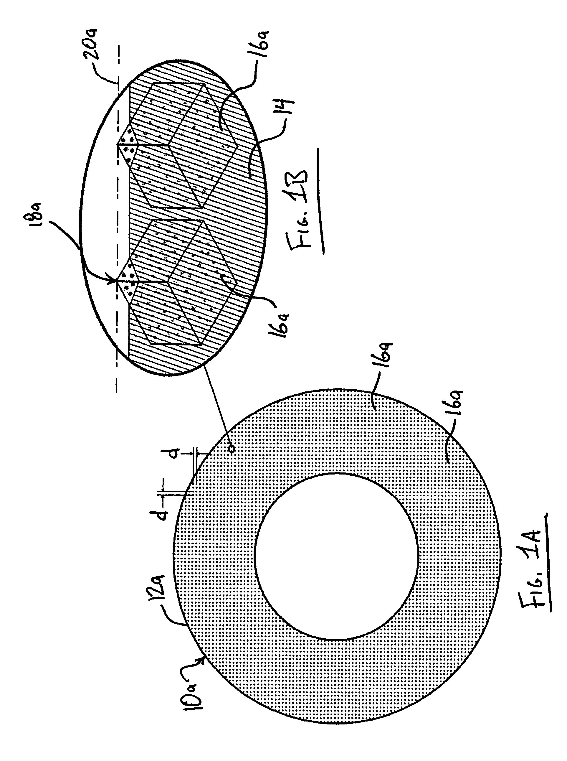
[0110]Individual sintered polycrystalline diamond cubes with silicon / SiC as the matrix were used as the cutting elements for forming a CMP pad conditioner. Each of the cubes contains about 90 V % of diamond (about 10 microns in grain size) and the remaining phase is either silicon or SiC. A very small amount of titanium is also present to facilitate the sintering process. The cubes were pressed in a graphite mold and were formed in a size of about 1 mm on each side.

[0111]An epoxy mold was provided with cavities configured to receive one apex of the PCD cubes. A parting layer was spread on top of the mold. Subsequently, another epoxy is cast on the top in vacuum. After curing, the mold is removed, exposing the apex of each cube. The apexes become the cutting tip of a pad conditioner.

example 2

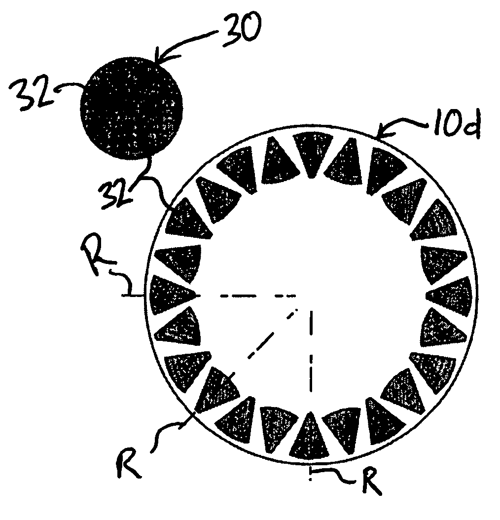
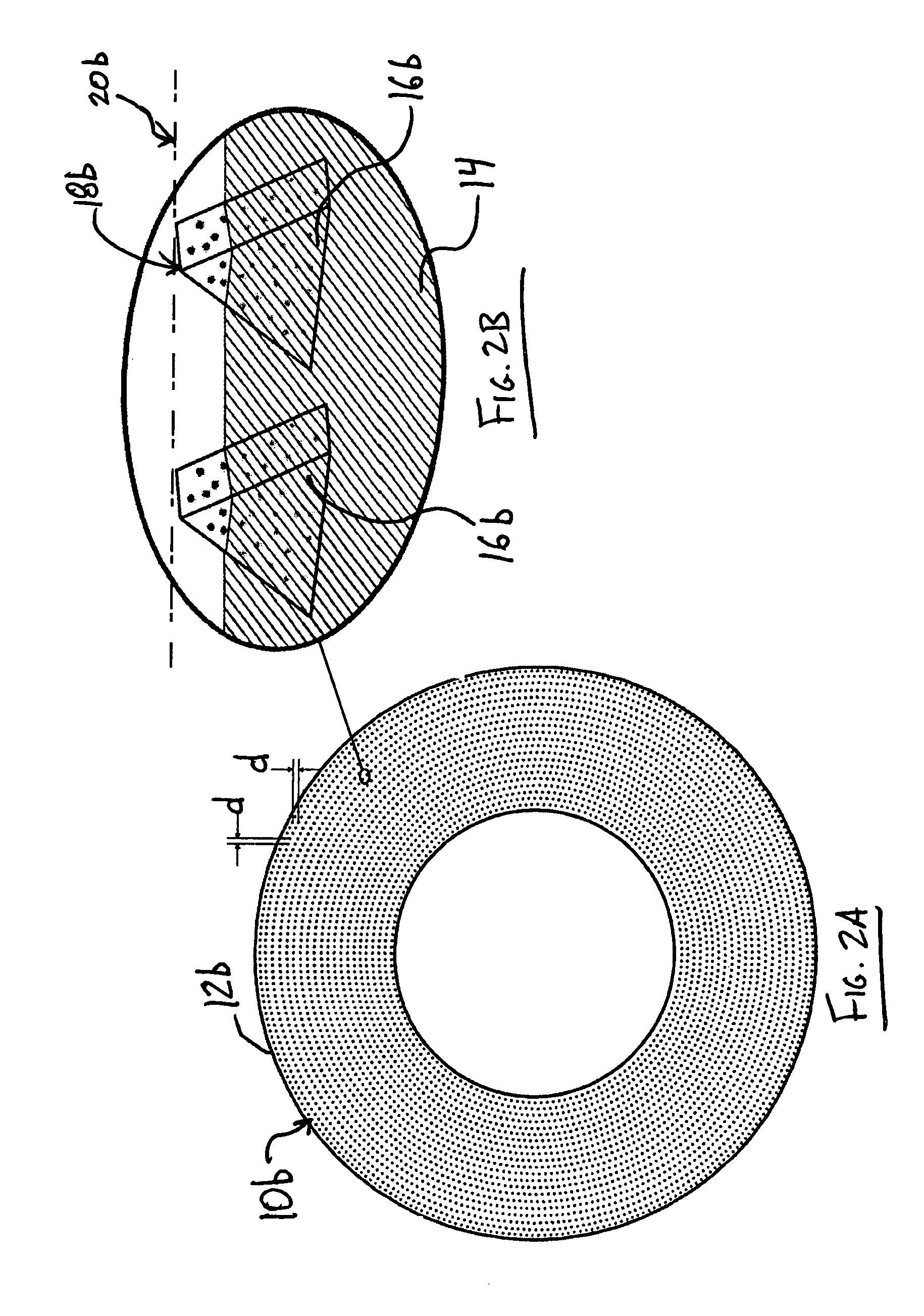
[0112]A disk of sintered polycrystalline diamond with silicon / SiC as the matrix is divided into a series of wedges of substantially the same volume. The wedges are used as the cutting elements for forming a CMP pad conditioner. Each of the wedges contains about 90 V % of diamond (about 10 microns in grain size) and the remaining phase is either silicon or SiC. A very small amount of titanium is also present to facilitate the sintering process.

[0113]An epoxy mold was provided with cavities configured to receive each of the PCD wedges. A parting layer was spread on top of the mold. Subsequently, another epoxy is cast on the top in vacuum. After curing, the mold is removed, exposing the face of each wedge. The faces (and edges of the faces) of the wedges become the cutting elements of a pad conditioner.

example 3

[0114]PCD blanks pressed from a cubic press were trimmed from both sides to remove refractary metal container (e.g. Ta). The outside diameter of the blanks were ground off. The PCD blanks were bonded to a cemented WC base and the PCD layer was EDM shaped to form pyramids distributed in a predetermined pattern. The PCD blanks were subsequently divided into a series of wedge-shaped cutting pieces and the cutting pieces were placed on a flat mold with the cutting pieces leveled with the mold.

[0115]The mold was placed in a vacuum chamber and epoxy is poured over the top. Finally, a stainless steel plate was placed on the top of the flowing epoxy and pressed toward the PCD until only a thin layer of epoxy remained between the backing of the PCD and the steel substrate. After curing of the epoxy, the PCD cutting tool was cleaned and mounting structure (e.g., holes) was formed on the back of the steel substrate.

[0116]The PCT cutting pieces can be arranged on the stainless steel plate in an...


PUM

PropertyMeasurementUnit
distanceaaaaaaaaaa
distanceaaaaaaaaaa
cutting depthaaaaaaaaaa

Abstract

A cutting device comprises a plurality of individual polycrystalline cutting elements secured in a solidified organic material layer. Each of the plurality of individual polycrystalline cutting elements has a substantially matching geometric configuration.

Description

PRIORITY DATA[0001]This application is a continuation-in-part of U.S. patent application Ser. No. 11 / 560,817, filed Nov. 16, 2006, which is a continuation-in-part of U.S. patent application Ser. No. 11 / 357,713, filed Feb. 17, 2006, which claims the benefit of U.S. Provisional Patent Application Ser. No. 60 / 681,798, filed May 16, 2005; and is also a continuation-in-part of U.S. patent application Ser. No. 11 / 223,786, filed Sep. 9, 2005; and is also a continuation-in-part of U.S. patent application Ser. No. 10 / 925,894, filed Aug. 24, 2004, all of which are hereby incorporated herein by reference in their entirety.FIELD OF THE INVENTION[0002]The present invention relates generally to cutting devices used to remove material from (e.g., plane, smooth, polish, dress, etc.) workpieces formed of various materials. Accordingly, the present invention involves the fields of chemistry, physics, and materials science.BACKGROUND OF THE INVENTION[0003]It is estimated that the semiconductor industr...

Claims


Application Information

Patent Timeline
Patent Type & Authority Patents(United States)
IPC IPC(8): B24B1/00
CPCB24B53/017B24B53/12B24D3/14
Inventor SUNG, CHIEN-MIN
Owner KINIK
Why Eureka
Try Eureka