Semiconductor device with a diffusion barrier film having a spacing for stress relief of solder bump

a diffusion barrier film and semiconductor chip technology, applied in semiconductor devices, semiconductor/solid-state device details, electrical devices, etc., can solve the problems of not having a higher structural strength, reducing the stress level of the above-described structure, and avoiding a single point concentration of stress, so as to reduce the stress level of the junction provided with the diffusion barrier film, the effect of avoiding the concentration of stress in a single point and reducing the stress concentration

Active Publication Date: 2010-02-16
RENESAS ELECTRONICS CORP
View PDF8 Cites 10 Cited by
  • Summary
  • Abstract
  • Description
  • Claims
  • Application Information

AI Technical Summary

Benefits of technology

[0024]Since this configuration provides dividing the junction between the diffusion barrier film and the bump into a plurality of small areas, the thermal stress exerted on the junction is effectively dispersed to each of the small areas, thereby avoiding a concentration the stress in a single point.
[0025]While a stress is generally concentrated in a circumference of a junction of a diffusion barrier film with a bump, the configuration of the present invention provides a considerably reduced level of such stress concentration as compared with the conventional configuration. The aspect of the present invention achieves that a thermal stress created in the junction provided with the diffusion barrier film is considerably reduced.
[0026]As described above, according to the present invention, a semiconductor device, which is configured to be provided with a diffusion barrier film having a geometry of including a spacing on an electrode coupled to the bump, can be obtained. Thus, the stress created in the diffusion barrier film can be effectively dispersed and relaxed. Accordingly, a semiconductor device having an improved reliability and providing an inhibition to causing an adverse effect over the electrode and the semiconductor chip is provided.

Problems solved by technology

However, a thermal stress is caused by a difference in thermal expansion coefficients of materials of respective components such as the semiconductor chip and the mounting substrate and the like in the CSP having such miniaturized solder-joint, as shown in FIG. 11, strain may be possibly concentrated on the solder-bump junction, which has not higher structural strength.
In this case, in the conventional structure, the stress tends to be concentrated in particular on the circumference portion of the contacting surface between the ball bump and the UBM, when one piece of hard disc-shaped the UBM repeatedly moves, and therefore a crack may be possibly generated in an aluminum electrode provided under the UBM or in the semiconductor chip.
However, relaxation of the stress by employing the above-described structure is strictly limited.
Further, the present inventors have also concluded that, the contact area between the bump and the UBM is not sufficiently smaller since a length of a side of the UBM along the stress direction is larger, even if the stress is exerted to the UBM from any direction, and thus the stress remains in an end of the UBM, even though the UBM is formed to have a corrugated geometry as in the technology described in Japanese Patent Laid-Open No. 2000-299,343, and therefore efficient relaxation of the stress created in the UBM is limited.
Further, although it is required to provide a broader width of the frame of the insulating film in order to reduce the stress transferred to the external of the opening region through the inside of the UBM, the broader width of the frame may possibly cause an increase in the area of the electrode and / or an increase in the contact resistance between the UBM and the metallic electrode.

Method used


Image

  • Semiconductor device with a diffusion barrier film having a spacing for stress relief of solder bump
  • Semiconductor device with a diffusion barrier film having a spacing for stress relief of solder bump
  • Semiconductor device with a diffusion barrier film having a spacing for stress relief of solder bump

Examples


Embodiment Construction

[0042]The invention will be now described herein with reference to illustrative embodiments. Those skilled in the art will recognize that many alternative embodiments can be accomplished using the teachings of the present invention and that the invention is not limited to the embodiments illustrated for explanatory purposed.

[0043]First embodiments according to the present invention will be described as follows in further detail, in reference to FIG. 1 to FIG. 5. In all figures, identical numeral is assigned to an element commonly appeared in the figures, and the detailed description thereof will not be presented.

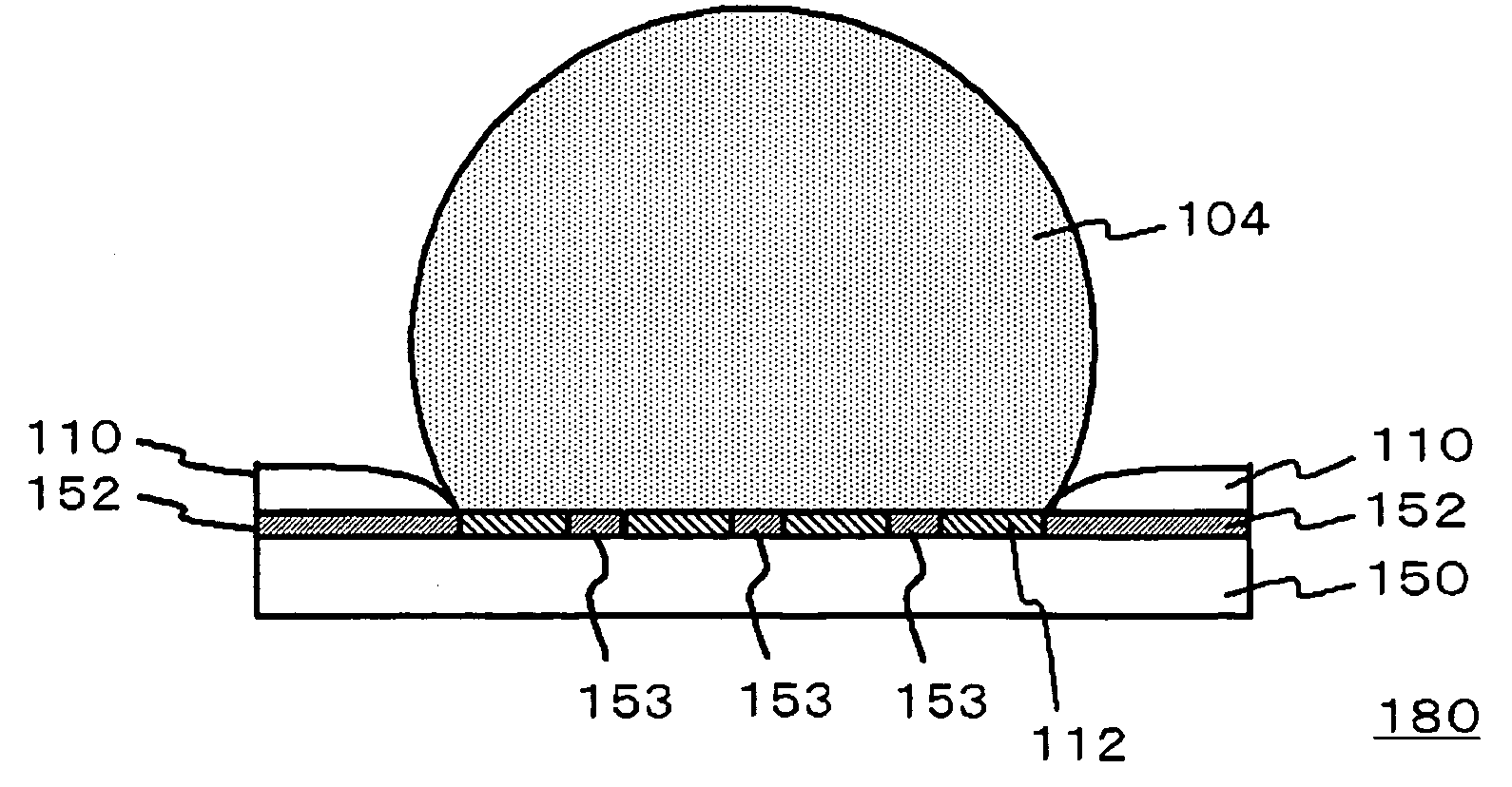
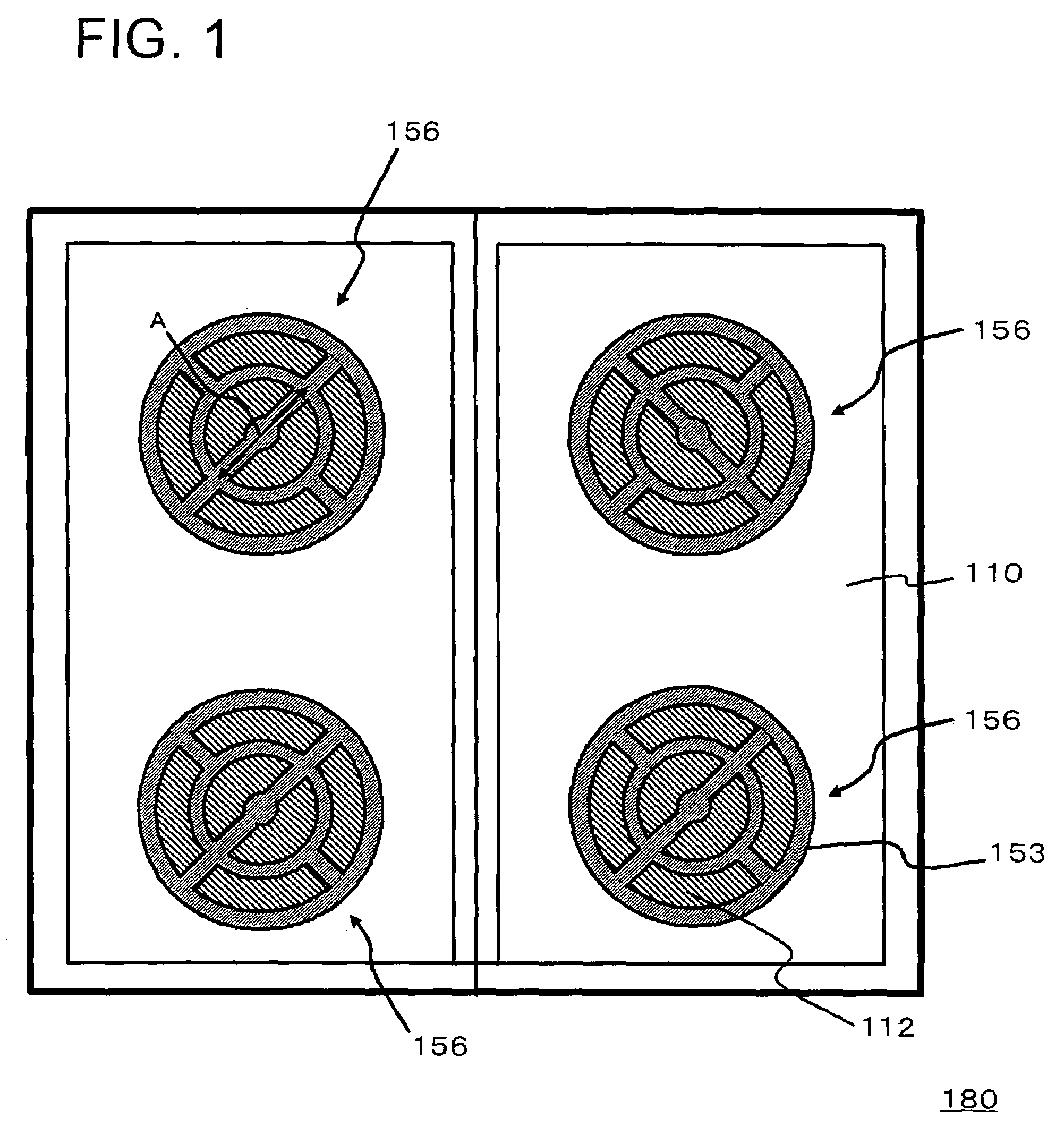
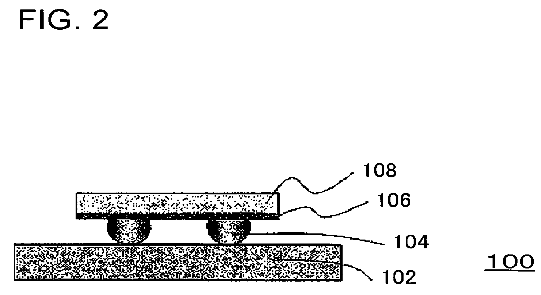
[0044]A semiconductor device 100 shown in FIG. 1 and FIG. 2 comprises a semiconductor chip 108 and a mounting substrate 102, and the semiconductor chip 108 is coupled to the mounting substrate 102 through bumps (solder bumps 104).

[0045]The semiconductor chip 108 includes electrodes (aluminum electrodes 150) in a surface thereof that is coupled to a mounting substrate 102, an...


PUM


Abstract

The present invention provides a semiconductor device exhibiting an improved reliability. A semiconductor device comprises a semiconductor chip having an electrode on a surface thereof and a mounting substrate, and the electrode (aluminum electrode) of the semiconductor chip is coupled to the mounting substrate through a bump (solder bump 104). A plurality of diffusion barrier films (UBM 112) for preventing a diffusion of a material composing the bump is provided between the electrode and the bump, and the diffusion barrier film is formed to have a plurality of divided portions via spacings therebetween.

Description

[0001]This application is based on Japanese patent application Nos. 2005-171,317 and 2006-133823, the contents of which are incorporated hereinto by reference.BACKGROUND OF THE INVENTION[0002]1. Field of the Invention[0003]The present invention relates to a semiconductor device having a semiconductor chip and a mounting substrate, which are mutually coupled via a bump.[0004]2. Related Art[0005]Typical structure of a conventional semiconductor chip is formed by wire-bonding an electrode provided on the semiconductor chip with a terminal lead disposed in a peripheral of a package and packaging the chip with an encapsulating resin.[0006]Since maximum number of the terminal leads that can be mounted on the substrate is limited under the circumstances of requiring reduced spacing between the terminal leads for increasing number of the terminals in one semiconductor chip in the packaging process for such structure, it is inevitable to increase the dimension of the package for maintaining ...

Claims


Application Information

Patent Timeline
Patent Type & Authority Patents(United States)
IPC IPC(8): H01L21/44H01L21/4763H01L29/40
CPCH01L24/05H01L24/03H01L24/16H01L24/12H01L2224/03H01L2224/0401H01L2224/13099H01L2924/01004H01L2924/01005H01L2924/01013H01L2924/01014H01L2924/01028H01L2924/01029H01L2924/01047H01L2924/01074H01L2924/01078H01L2924/01082H01L2924/014H01L2924/05042H01L2924/01006H01L2924/01033H01L2224/05551H01L2224/02123H01L2224/05557H01L2224/05576H01L2224/16227H01L2924/351H01L2924/00
Inventor YAMADA, YUKIKO
Owner RENESAS ELECTRONICS CORP
Why Eureka
Try Eureka