Film formation apparatus, method for forming film, and method for manufacturing photoelectric conversion device

a technology film formation apparatus, which is applied in the direction of plasma technique, sustainable manufacturing/processing, and final product manufacturing, etc., can solve the problems of difficult use of photoelectric conversion device as a product, reduced yield, and adverse effects of light to be received, so as to prevent damage to the light receiving region of an element, suppress curling, and highly reliable photoelectric conversion device

Inactive Publication Date: 2010-02-23
SEMICON ENERGY LAB CO LTD
View PDF20 Cites 11 Cited by
  • Summary
  • Abstract
  • Description
  • Claims
  • Application Information

AI Technical Summary

Benefits of technology

[0009]It is an object of the present invention to suppress occurrence of a curled substrate in film formation and provide a highly reliable photoelectric conversion device by suppressing occurrence of damage in a light receiving region, thereby obtaining a photoelectric conversion device with high reliability.
[0026]In the present invention, a film is formed over a surface opposite to a light receiving region over a substrate so that a touch roller is in contact with a film formation surface. Thus, damage to the light receiving region of an element can be prevented. Therefore, a highly reliable photoelectric conversion device can be obtained.
[0027]In accordance with the present invention, occurrence of curl can be suppressed in a boundary between a region where a film is formed and a region where a film is not formed. Thus, damage to a light receiving region of an element can be prevented.
[0028]In accordance with the present invention, curling of a substrate can be suppressed, so that a substrate can be transferred smoothly. Therefore, a film formation apparatus having high stability for transfer can be obtained.

Problems solved by technology

When the substrate 1018 is curled, a photoelectric conversion device may be difficult to be used as a product and a yield may be reduced.
Further, if the rear surface of the substrate 1018 is damaged by the touch rollers, light to be received may have adverse effect, or appearance quality may be deteriorated in being incorporated into a product.

Method used


Image

  • Film formation apparatus, method for forming film, and method for manufacturing photoelectric conversion device
  • Film formation apparatus, method for forming film, and method for manufacturing photoelectric conversion device
  • Film formation apparatus, method for forming film, and method for manufacturing photoelectric conversion device

Examples


embodiment mode 1

[0061]This embodiment mode will be explained with reference to FIGS. 1A to 1C, FIG. 3, FIGS. 4A to 4C, and FIGS. 5A and 5B.

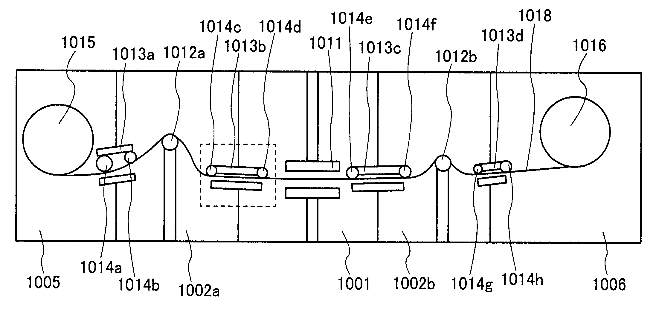
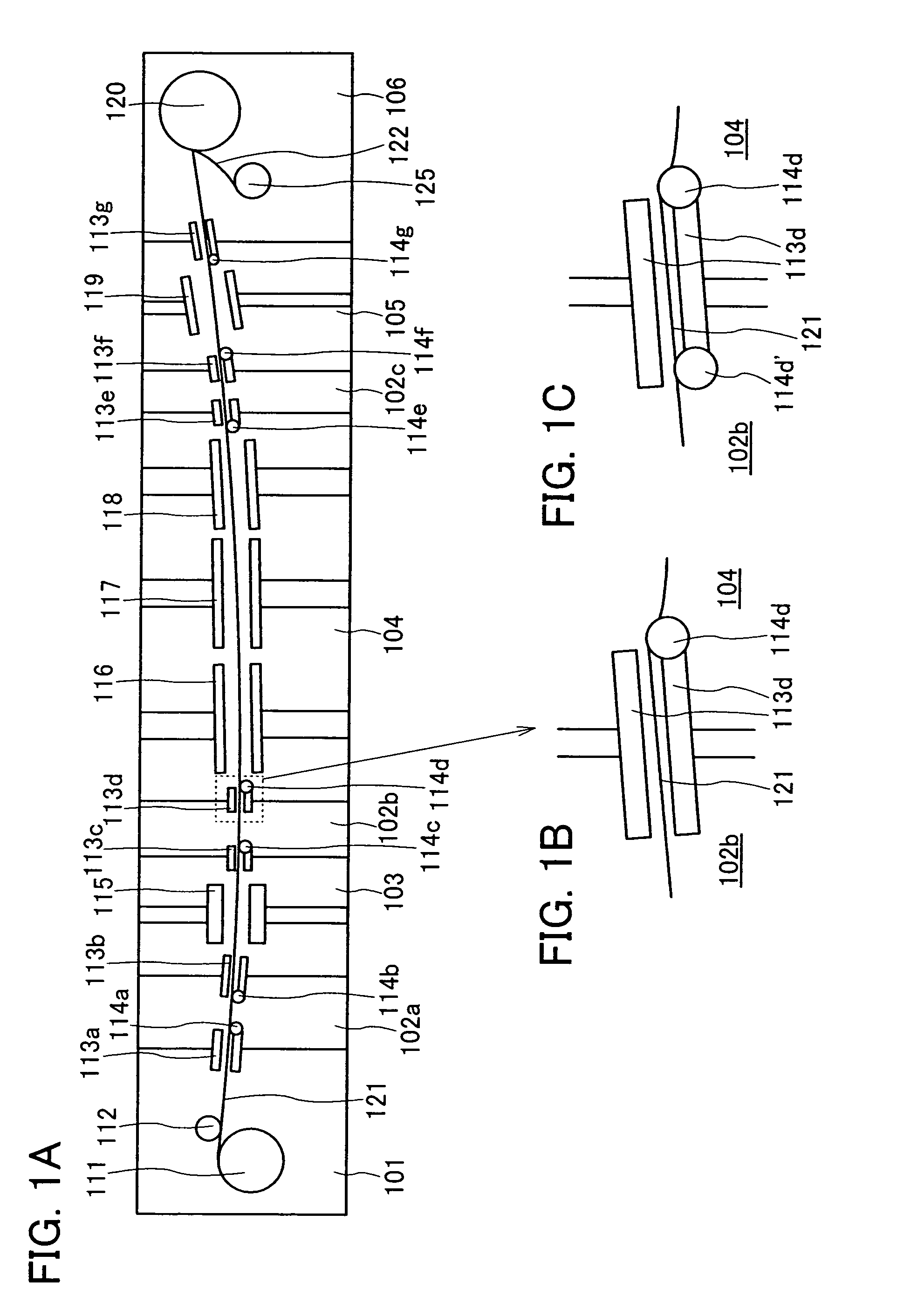
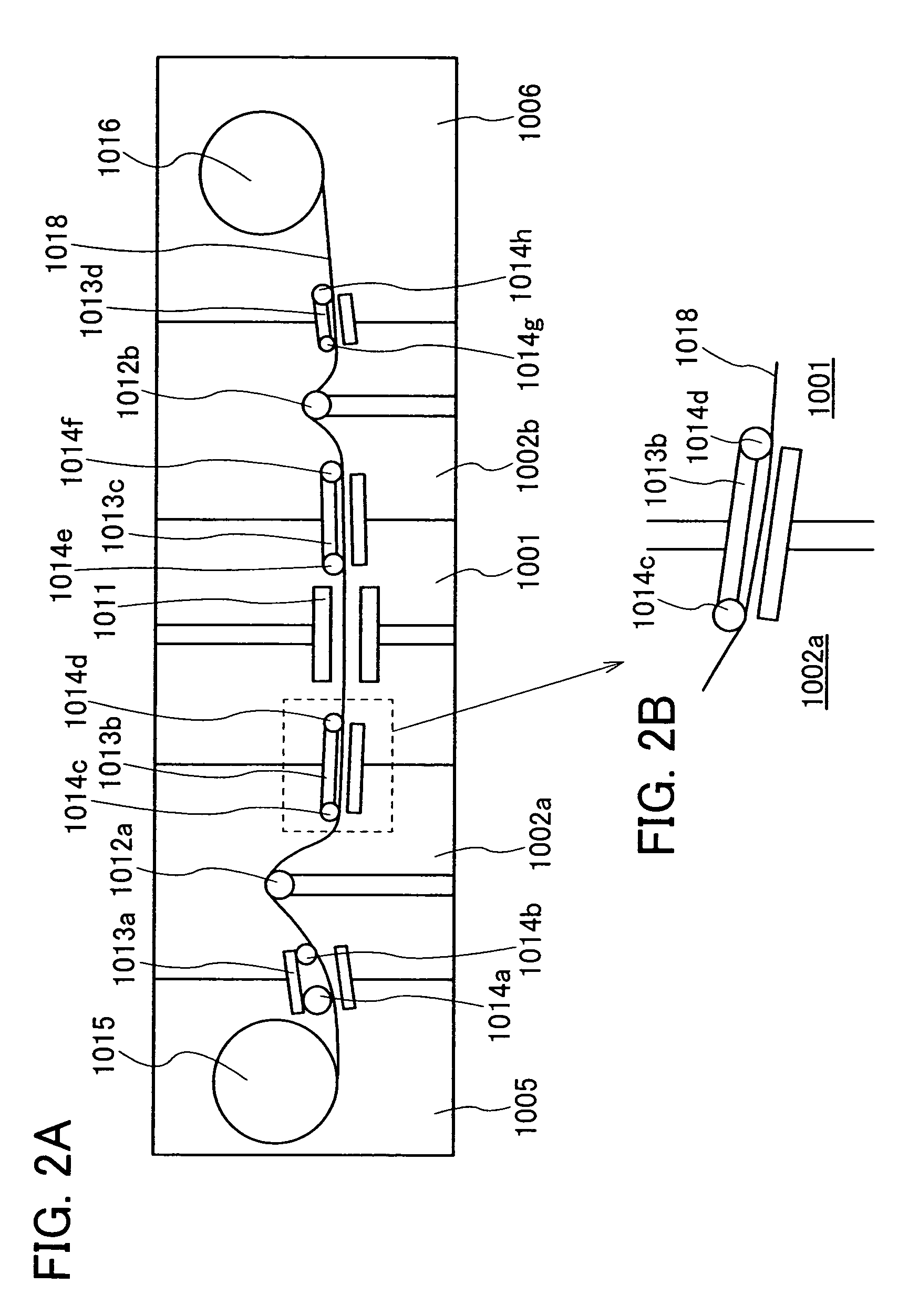
[0062]FIG. 1A shows an overall view of a film formation apparatus of this embodiment mode, and FIGS. 1B and 1C show views of an enlarged slit and touch roller. The film formation apparatus shown in FIG. 1A includes transfer chambers 101 and 106, buffer chambers 102 (102a, 102b, and 102c), and film formation chambers 103, 104, and 105.

[0063]In the transfer chamber 101, a roller 111 and a touch roller 112 for sending a substrate 121 are provided. The substrate 121 is a flexible substrate, and for example, a polyethylene naphthalate (PEN) film, a polyethylene terephthalate (PET) film, a polybutylene naphthalate (PBN) film, or the like may be used. The substrate 121 is sent from the roller 111 to the buffer chamber 102.

[0064]The buffer chamber 102 is provided between the transfer chamber and the film formation chamber or between the film formation chambers. By trans...

embodiment mode 2

[0094]In this embodiment mode, an example of a different structure of the film formation chamber 104 in FIGS. 1A to 1C from that of Embodiment Mode 1 will be explained with reference to FIG. 6 and FIG. 7.

[0095]FIG. 6 shows a state in which a substrate 121 is transferred between upper electrodes 301 (301a, 301b, and 301c) and lower electrodes 302 (302a, 302b, and 302c) of a discharging electrode provided in a film formation chamber. Masks 304 (304a, 304b, and 304c) are provided between the substrate 121 and the lower electrodes 302. In other words, the lower electrode 302a is provided with the mask 304a, the lower electrode 302b is provided with the mask 304b, and the lower electrode 302c is provided with the mask 304c.

[0096]The upper electrode 301 is divided into a plurality of upper electrodes, for example, three upper electrodes 301a, 301b, and 301c, each of which has a roll electrode 303. In other words, the upper electrode 301a is provided with the roll electrodes 303a (303aa, ...

embodiment 1

[0103]In this embodiment, a method for manufacturing a solar battery by the present invention will be explained with reference to FIGS. 8A to 8C, FIGS. 9A to 9C, FIG. 10, FIGS. 11A to 11C, FIG. 12, and FIGS. 13A and 13B.

[0104]In FIG. 8A, as for a substrate 401, an organic resin material such as polyethylene terephthalate (PET), polyethylene naphthalate (PEN), polyether sulfone (PES), or polybutylene naphthalate (PBN) is used. In this embodiment, polyethylene naphthalate (PEN) with a thickness of 60 to 100 μm is used as the substrate 401.

[0105]A solar battery manufactured in this embodiment is an integrated solar battery in which a plurality of unit cells is connected in series over the same substrate. Further, the solar battery of this embodiment has a structure in which light is received in a surface opposed to a surface over which a photoelectric conversion layer is formed over the substrate 401. A transparent electrode layer 402 is first formed over the substrate 401. The transpa...


PUM

PropertyMeasurementUnit
grain sizeaaaaaaaaaa
energy bandaaaaaaaaaa

Abstract

The present invention relates to a film formation apparatus including a first transfer chamber having a roller for sending a substrate, a film formation chamber having a discharging electrode, a buffer chamber provided between the transfer chamber and the film formation chamber or between the film formation chambers, a slit provided in a portion where the substrate comes in and out in the buffer chamber, and a second transfer chamber having a roller for rewinding the substrate. The slit is provided with at least one touch roller, and the touch roller is in contact with a film formation surface of the substrate. In addition, the present invention also relates to a method for forming a film and a method for manufacturing a photoelectric conversion device that are performed by using such a film formation apparatus.

Description

BACKGROUND OF THE INVENTION[0001]1. Field of the Invention[0002]The present invention relates to a photoelectric conversion element, a photoelectric conversion device, and a method for manufacturing the same. Further, the present invention also relates to an electronic appliance and a semiconductor device using a photoelectric conversion device.[0003]2. Description of the Related Art[0004]In recent years, a process in which a photoelectric conversion device can be manufactured at low cost has been expected. As one of methods for attempting low cost manufacture, a method has been known, by which each unit operation such as film formation, printing, or laser processing is continuously processed in a process where a rolled flexible substrate is rewound to another roll. This method is referred to as a Roll-to-Roll method (refer to Patent Document 1: Japanese Published Patent Application No. 2001-223375).[0005]FIGS. 2A and 2B show a film formation apparatus for a conventional Roll-to-Rol...

Claims


Application Information

Patent Timeline
Patent Type & Authority Patents(United States)
IPC IPC(8): H01L21/20C23C16/54
CPCC23C16/24C23C16/458C23C16/545H01L31/202H05H1/24Y02E10/50H05H1/2406Y02P70/50H05H1/2431H05H1/473
Inventor HIURA, YOSHIKAZUADACHI, HIROKITAKAHASHI, HIRONOBUSUGAWARA, YUUSUKEARAO, TATSUYANISHI, KAZUOARAI, YASUYUKI
Owner SEMICON ENERGY LAB CO LTD
Why Eureka
Try Eureka