Semiconductor device

a technology of semiconductors and components, applied in the direction of semiconductor devices, electrical devices, transistors, etc., can solve the problems of reducing the degree of integration of elements, so as to achieve the effect of increasing reducing the degree of integration, and reducing the number of manufacturing steps

Inactive Publication Date: 2010-02-23
ABLIC INC
View PDF3 Cites 2 Cited by
  • Summary
  • Abstract
  • Description
  • Claims
  • Application Information

AI Technical Summary

Benefits of technology

[0013]According to the present invention, As described above, a semiconductor device can be obtained in which the number of the manufacturing steps is not increased, enough latch-up resistance is secured for the high power supply voltage circuit section, the low power supply voltage circuit section uses the same trench isolation structure as that of the high power supply voltage circuit section, and still, the degree of integration is high.

Problems solved by technology

Accordingly, there is a problem that, when the low power supply voltage circuit sections use the same trench isolation as that of the high power supply voltage circuit sections, the degree of integration of elements reduces in the low power supply voltage sections to which high degree of integration is required.
Accordingly, there is a problem that, when the low power supply voltage circuit section uses the same trench isolation as that of the high power supply voltage circuit section, the degree of integration of elements reduces in the low power supply voltage section to which high degree of integration is required.
The examples in which the depth of a well in the high power supply voltage circuit section is made larger than that of a well in the low power supply voltage circuit section and the width of a trench isolation portion in the high power supply voltage circuit section is made larger than that in the low power supply voltage circuit section have been proposed, however, there are problems that the number of the manufacturing steps increases and that the increase in the width of a trench isolation portion leads to increase in cost.

Method used


Image

  • Semiconductor device
  • Semiconductor device
  • Semiconductor device

Examples


embodiment 1

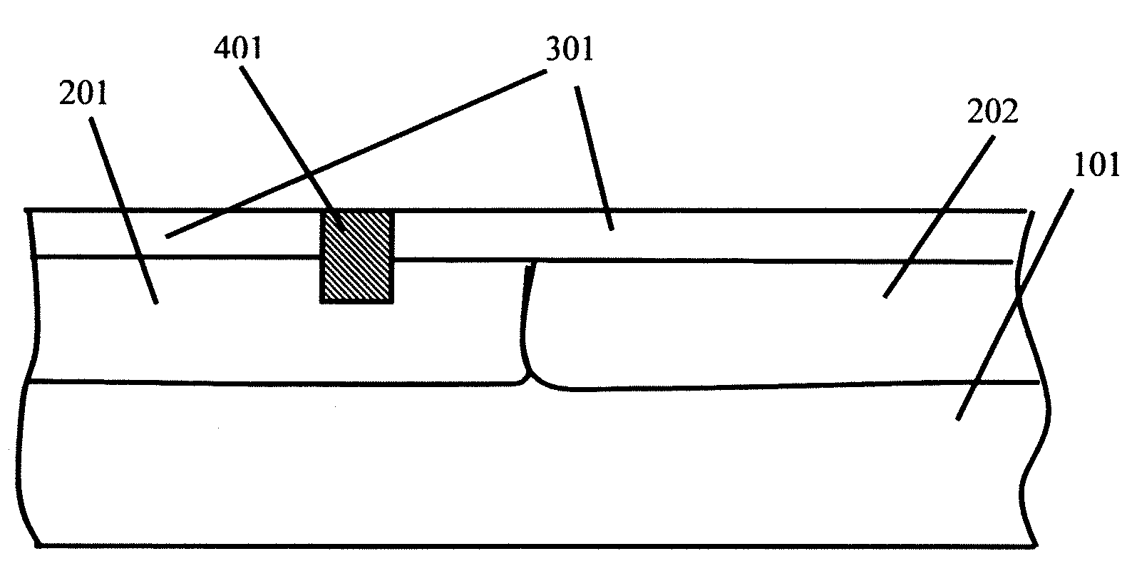
[0018]FIG. 1 is a schematic sectional view illustrating a first embodiment of a high power supply voltage circuit section in a semiconductor device according to the present invention.

[0019]A P-type well region 201 which is a low concentration P-type impurity region as a first well and an N-type well region 202 which is a low concentration N-type impurity region as a second well are formed so as to be adjacent to each other on a P-type silicon substrate 101 as a semiconductor substrate of a first conductivity type. A plurality of MOS transistors (not shown) is formed on surfaces of the wells, and a trench isolation region 301 for isolating the MOS transistors is formed. A part of the trench isolation region 301 in the P-type well region 201 in the vicinity of a junction between the P-type well region 201 and the N-type well region 202 is removed and a carrier capture region 401 which is a high concentration P-type impurity region and has the depth larger than that of the trench isola...

embodiment 2

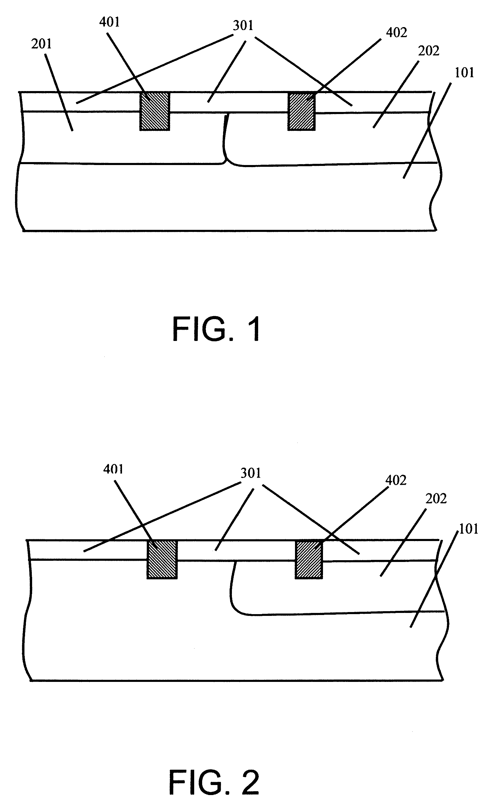
[0026]FIG. 2 is a schematic sectional view illustrating a second embodiment of a high power supply voltage circuit section in a semiconductor device according to the present invention.

[0027]An N-type well region 202 which is a low concentration N-type impurity region as a second well is formed on a P-type silicon substrate 101 as a semiconductor substrate of a first conductivity type. A plurality of MOS transistors (not shown) is formed on their surfaces, and a trench isolation region 301 for isolating the MOS transistors is formed. A part of the trench isolation region 301 in the P-type silicon substrate 101 in the vicinity of a junction between the P-type silicon substrate 101 and the N-type well region 202 is removed and a carrier capture region 401 which is a high concentration P-type impurity region and has the depth larger than that of the trench isolation region 301 is formed. A part of the trench isolation region 301 in the N-type well region 202 is also removed and a carrie...

embodiment 3

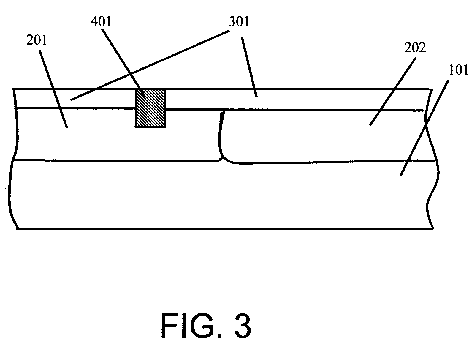
[0032]FIG. 3 is a schematic sectional view illustrating a third embodiment of a high power supply voltage circuit section in a semiconductor device according to the present invention.

[0033]A P-type well region 201 which is a low concentration P-type impurity region as a first well and an N-type well region 202 which is a low concentration N-type impurity region as a second well are formed so as to be adjacent to each other on a P-type silicon substrate 101 as a semiconductor substrate of a first conductivity type. A plurality of MOS transistors (not shown) is formed on their surfaces, and a trench isolation region 301 for isolating the MOS transistors is formed. A part of the trench isolation region 301 in the P-type well region 201 in the vicinity of a junction between the P-type well region 201 and the N-type well region 202 is removed and a carrier capture region 401 which is a high concentration P-type impurity region and has the depth larger than that of the trench isolation re...


PUM


Abstract

Provided is a semiconductor device having a trench isolation structure and a high power supply voltage circuit section including at least a well region and a MOS transistor formed therein. The high power supply voltage circuit section includes a carrier capture region for preventing latch-up in a vicinity of an end portion of the well region, and a depth of the carrier capture region is larger than a depth of the trench isolation region. The carrier capture region in the high power supply voltage circuit section is formed of a diffusion layer which is the same as that of a source or a drain region of the MOS transistor formed in the high power supply voltage circuit section.

Description

REFERENCE TO THE RELATED APPLICATIONS[0001]This application claims priority under 35 U.S.C. §119 to Japanese Patent Application No. JP2007-032034 filed Feb. 13, 2007, the entire content of which is hereby incorporated by reference.BACKGROUND OF THE INVENTION[0002]1. Field of the Invention[0003]The present invention relates to a semiconductor device having a trench isolation structure. More particularly, the present invention relates to a semiconductor device such as a CMOS device having multiple power supply voltages and using trench isolation for element isolation structure.[0004]2. Description of the Related Art[0005]In a semiconductor device having CMOS devices which use multiple power supply voltages, it is important to improve degree of integration of low power supply voltage sections forming an internal circuit such as a logic circuit and, at the same time, to secure latch-up resistance of high power supply voltage sections used for input / output circuits or the like.[0006]Elem...

Claims


Application Information

Patent Timeline
Patent Type & Authority Patents(United States)
IPC IPC(8): H01L29/76H01L29/94H01L31/062H01L21/822H01L21/8238H01L27/04H01L27/08H01L27/088H01L27/092
CPCH01L27/0921H01L21/823412H01L21/823481H01L21/823493
Inventor TAKASU, HIROAKIINOUE, NAOTOYAMAMOTO, SUKEHIRO
Owner ABLIC INC
Why Eureka
Try Eureka