
Device and method for reducing input noise

a technology of input noise and device, applied in the field of devices and methods for reducing input noise, can solve the problems of button bouncing, poor contact and usage wear, and considerable noise generation, and achieve the effect of reducing input nois

Active Publication Date: 2010-03-02
HOLTEK SEMICON
View PDF3 Cites 0 Cited by
  • Summary
  • Abstract
  • Description
  • Claims
  • Application Information

AI Technical Summary

Benefits of technology

"The present invention provides a device and method for reducing input noise in touch switches. The device includes a microcontroller with a noise reduction device, analog switch, control unit, signal output unit, and oscillation circuit. The method involves turning on or off the noise reduction device and analog switch to control the input of signals. The noise reduction device is connected to a potential to charge or discharge a plurality of charges stored in an equivalent capacitor when turned on. The technical effect of this invention is to improve the accuracy and reliability of touch switches by reducing input noise."

Problems solved by technology

However, such input devices have problems such as button bouncing, poor contacts and usage wear.
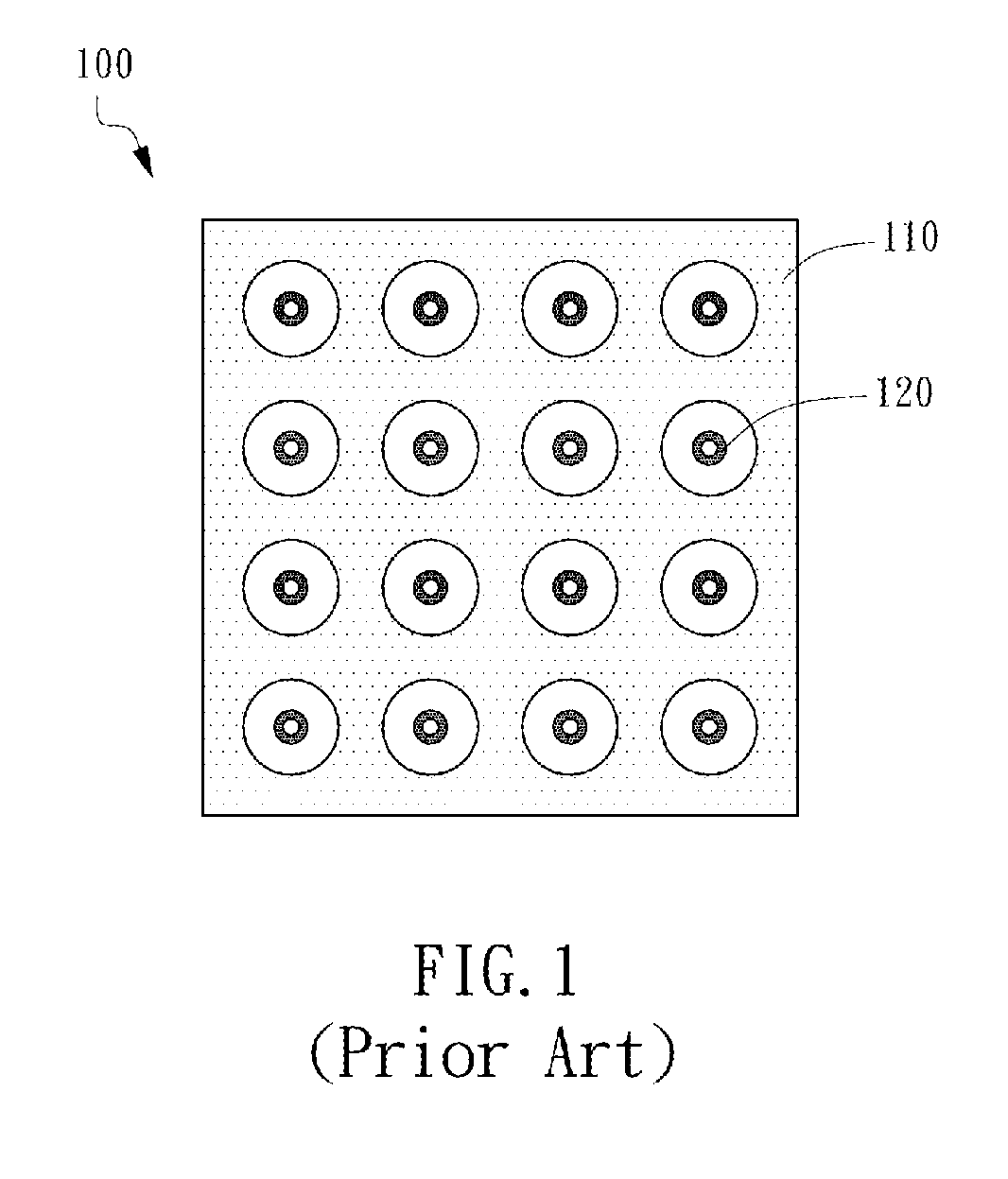
When the area is limited by the circuitry or structure, considerable noise is generated due to insufficient area for GND or VDD.
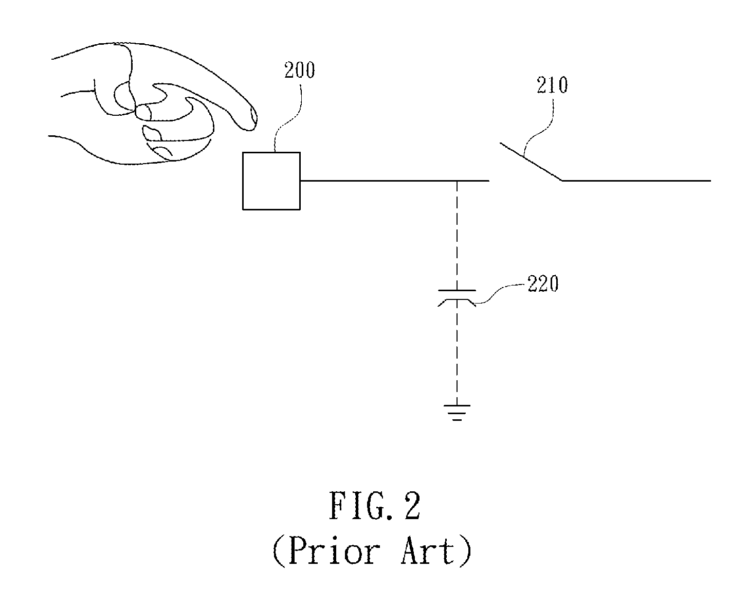
However, the aforesaid technology is not suitable for reducing input noise when the buttons are used as a user interface. FIG. 2 is an equivalent circuit showing an equivalent capacitor when the analog switch is turned off.
Because of the input noise, the user has to set the software parameters according to practical use.
Moreover, the error tolerance of the back-end timer / counter has to be larger, which leads to the need in a timer / counter of a larger number of bits.

Method used


Image

  • Device and method for reducing input noise
  • Device and method for reducing input noise
  • Device and method for reducing input noise

Examples


Embodiment Construction

[0034]The present invention providing a device for reducing input noise can be exemplified by the preferred embodiments as described hereinafter.

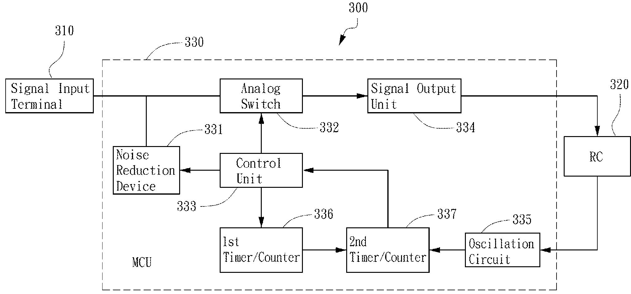
[0035]Please refer to FIG. 3, which is a block diagram of a device for reducing input noise according to one preferred embodiment of the present invention. In FIG. 3, the device for reducing input noise 300 comprises: at least a signal input terminal 310 (exemplified by but not limited to a touch panel or a touch switch); at least a RC circuit 320, which comprises at least a resistor and at least a capacitor; and at least a microcontroller 330. The microcontroller 330 comprises: at least a noise reduction device 331 (exemplified by but not limited to a metal-oxide-semiconductor field-effect transistor (MOSFET)) having one end being connected to the signal input terminal 310; at least an analog switch 332 (exemplified by but not limited to an analog switch), having one end being connected to the signal input terminal 310 and one end of the n...


PUM


Abstract

A device and a method for reducing input noise providing at least a microcontroller. The microcontroller comprises: at least a noise reduction device, at least an analog switch and at least a signal output unit. The noise reduction device connected to the ground or a voltage is turned on to charge or discharge a stray capacitor existing on a turned off analog switch so that the amount of charge stored in the stray capacitor is zero or a specific value. Thereby, the noise in a touch switch is reduced and the cost of layout on the PCB is saved.

Description

BACKGROUND OF THE INVENTION[0001]1. Field of the Invention[0002]The present invention generally relates to a device and a method for reducing input noise and, more particularly, to a device and a method for reducing input noise using a noise reduction device turned on and connected to a ground or a voltage so that a plurality of charges stored in an equivalent capacitor of a turned off analog switch are released or accumulated to zero or a specific value.[0003]2. Description of the Prior Art[0004]The conventional user interface uses mechanic buttons as its input devices. For example, the input devices for telephones, electronic calculators, induction cookers, electric rice cookers are implemented using buttons. However, such input devices have problems such as button bouncing, poor contacts and usage wear. Therefore, touch switches have become more and more popular due to the rapid advancement in development to overcome the problems related to mechanic buttons. In the process for ma...

Claims


Application Information

Patent Timeline
Patent Type & Authority Patents(United States)
IPC IPC(8): H03K5/00
CPCH03K5/1254
Inventor LIU, WEN-LIANGYANG, CHIN-HUNG
Owner HOLTEK SEMICON
Learn More