Electric connecting apparatus for semiconductor devices and contact used therefor

a technology of connecting apparatus and semiconductor devices, which is applied in the direction of electrical apparatus contruction details, coupling device connection, instruments, etc., can solve the problems of unstable contact position between the terminal portion of the plunger and the external contact point of the semiconductor device, risk of formation of contact marks on the side surface of the solder ball by the plunger, and inability to obtain predetermined contact pressure between the terminal portion and the external contact point. , to achieve the effect of avoiding damage to the external contact poin

Active Publication Date: 2010-03-16
YAMAICHI ELECTRONICS
View PDF91 Cites 43 Cited by
  • Summary
  • Abstract
  • Description
  • Claims
  • Application Information

AI Technical Summary

Benefits of technology

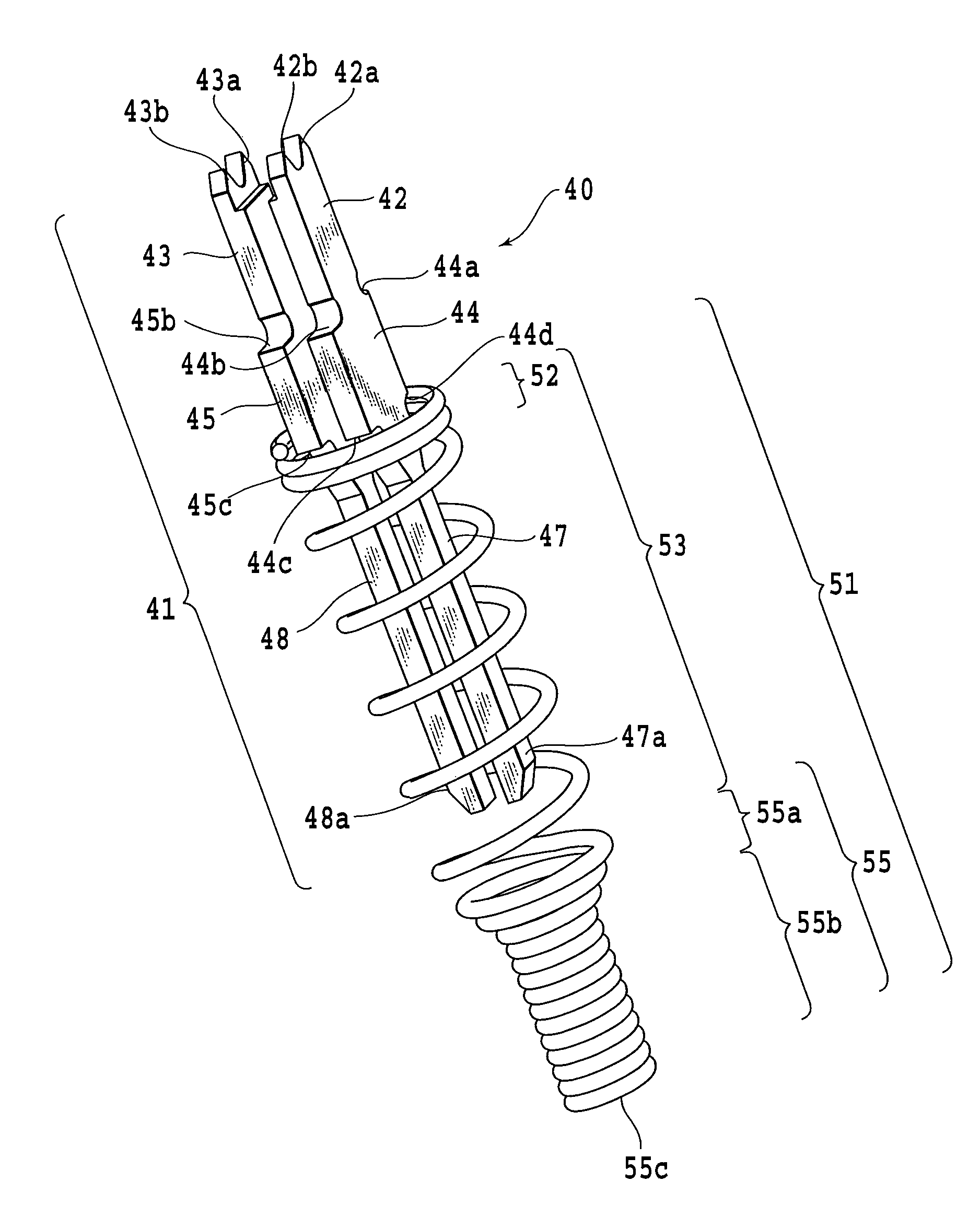
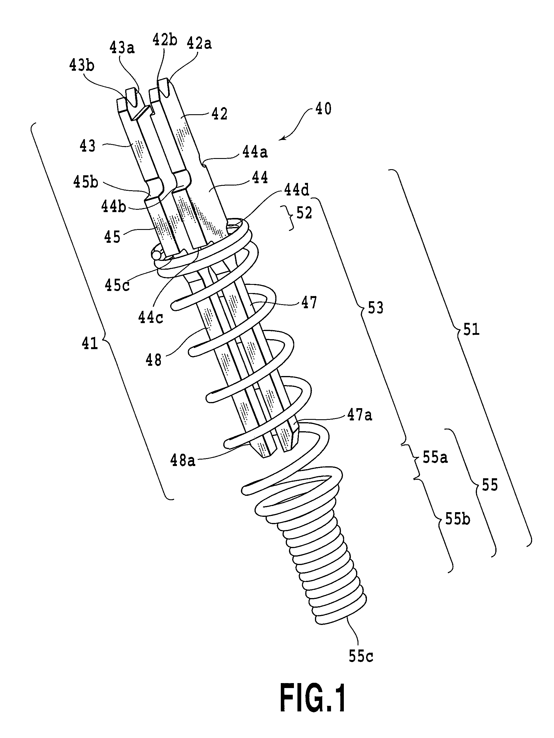
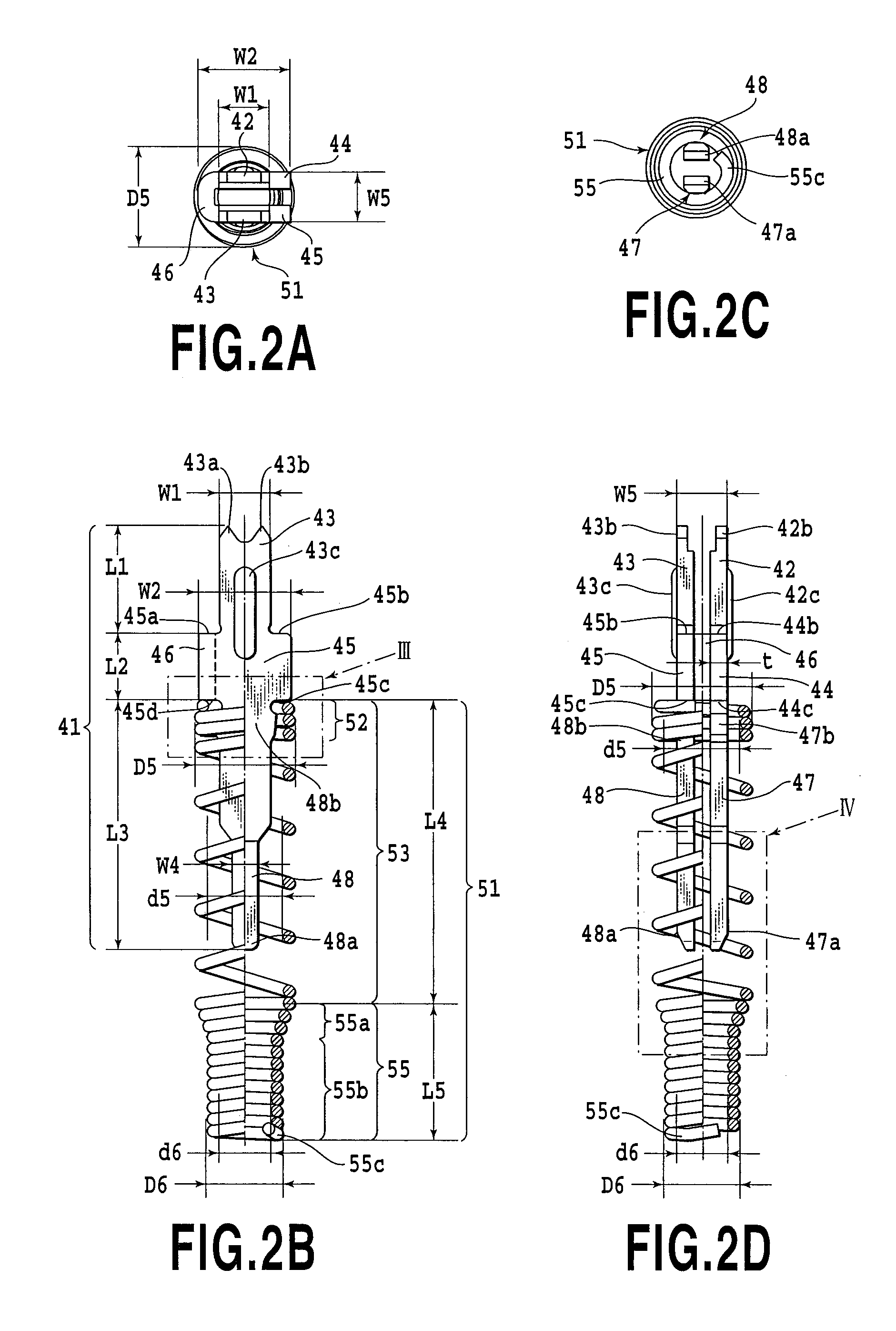
[0015]The contact according to the invention includes the two resiliently deformable contact strips provided on the lower contact strip of the plunger, so that the two contact strips reliably come into contact with the inner peripheral surface of the slimly wound portion of the coil sprint unit when the plunger is pressed downward. Therefore, when such contacts are built in the electric connecting apparatus, an electrically short-circuited path is formed on the each contact, so that the resistance of the path may be reduced, and a high-speed signal transmission is achieved, whereby a reliable electric connecting apparatus is provided.
[0016]Since the at lest three contact points are arranged on the upper end of the upper contact strip of the plunger in a plane so as to be broadened at a distance, the at least three contact points are electrically connected to the external contact point of the s...

Problems solved by technology

In this case, the contact position between the terminal portion of the plunger and the external contact point of the semiconductor device may be unstable due to the inclination of the plunger.
Therefore, when the contact at a predetermined contact position is not achieved, a predetermined contact pressure might not be obtained between the terminal portion and the external contact point due to an insufficient amount of displacement of the contact.
There is also a risk of formation o...

Method used


Image

  • Electric connecting apparatus for semiconductor devices and contact used therefor
  • Electric connecting apparatus for semiconductor devices and contact used therefor
  • Electric connecting apparatus for semiconductor devices and contact used therefor

Examples


first embodiment

[0056]First of all, a first embodiment of an IC socket according to the invention will be described. FIG. 5 shows a schematic drawing of an IC socket according to the invention.

[0057]As shown in FIG. 5, an IC socket 10 in the invention schematically includes a first base member 20, a second base member 30, and a plurality of contacts 40. Reference numeral 80 designates a second contacted object which comes into contact with the contacts 40 of the IC socket 10, which is a wiring substrate such as a test board on which the IC socket 10 is attached. Reference numeral 90 designates a first contacted object which comes into contact with the contacts 40 of the IC socket 10, which is an IC package to be mounted on the IC socket 10. The IC package 90 as the first contacted object is electrically connected to the wiring substrate 80 as the second contacted object via the IC socket 10. In this embodiment, the IC package 90 as the first contacted object includes a mold body 91 and a plurality ...


PUM


Abstract

The contact includes the plunger and a coil spring unit for holding the plunger thereon. The plunger includes an upper contact strip having a plurality of contact points on an upper end portion thereof, a wide portion, and a lower contact strip having two contact strips each having a contact point at a lower end portion thereof. The coil spring unit includes a spring portion and a funnel shaped tight wound portion including a guiding portion and a slimly wound portion having a contact point at a lower end portion thereof. The plurality of contact points provided on the upper contact strip is arranged in a plane so as to be broadened at a distance. The contact points provided on the two contact strips of the lower contact strip are formed to be resiliently deformable with respect to each other.

Description

[0001]This application claims the benefit of Japanese Patent Application No. 2008-333948, filed Dec. 26, 2008, which is hereby incorporated by reference herein in its entirety.BACKGROUND OF THE INVENTION[0002]1. Field of the Invention[0003]The present invention relates to an electric connecting apparatus for semiconductor devices configured to electrically connect semiconductor devices as a first contacted object, such as semiconductor wafer, bear chip, integrated circuit package, and liquid crystal display panel, with a wiring substrate as a second contacted object in order to conduct an inspection electrically, and a contact used therefor.[0004]2. Description of the Related Art[0005]In a process of manufacturing semiconductor devices such as semiconductor wafers, bear chips, integrated circuit packages (also referred to as “IC package”), and liquid crystal display panels (also referred to as “LCD panels”), various tests are conducted for inspecting the presence or absence of defec...

Claims


Application Information

Patent Timeline
IPC IPC(8): H01R12/00
CPCG01R1/0466G01R1/06722H01R13/2421H05K7/1069G01R1/0483G01R1/06738H01R2201/20H01R12/714H01R13/24G01R1/073
Inventor SUZUKI, KATSUMISUZUKI, TAKEYUKI
Owner YAMAICHI ELECTRONICS
Why Eureka
Try Eureka