Semiconductor device having copper metal line and method of forming the same

a technology of semiconductor devices and copper metal lines, which is applied in the direction of semiconductor devices, semiconductor/solid-state device details, electrical apparatus, etc., can solve the problems of reducing reliability, degrading electromigration (em) characteristics, and difficult etching of copper metal lines by an existing dry etch method, so as to prevent the degradation of electromigration (em) characteristics and improve reliability

Inactive Publication Date: 2010-03-16
DONGBU HITEK CO LTD
View PDF10 Cites 2 Cited by
  • Summary
  • Abstract
  • Description
  • Claims
  • Application Information

AI Technical Summary

Benefits of technology

[0014]It is, therefore, an object of the present invention to provide a method of forming a copper metal line in a semiconductor device, which is capable of improving a reliability by preventing the degradation of the electromigration (EM) characteristic, which is caused by poor adhesion and an unstable surface state between an insulating anti-diffusion film and a copper metal line.

Problems solved by technology

However, a copper metal line is difficult to be etched by an existing dry etch method.
However, since the copper metal and the SiN film have poor adhesion and form an unstable surface state, there are problems in that an electromigration (EM) characteristic is degraded and reliability is lowered.
Accordingly, there is a problem in that the reliability of a semiconductor device is degraded.

Method used


Image

  • Semiconductor device having copper metal line and method of forming the same
  • Semiconductor device having copper metal line and method of forming the same
  • Semiconductor device having copper metal line and method of forming the same

Examples


Embodiment Construction

[0037]Hereinafter, embodiments of the present invention will be described in detail with reference to the accompanying drawings so that they can be readily implemented by those skilled in the art.

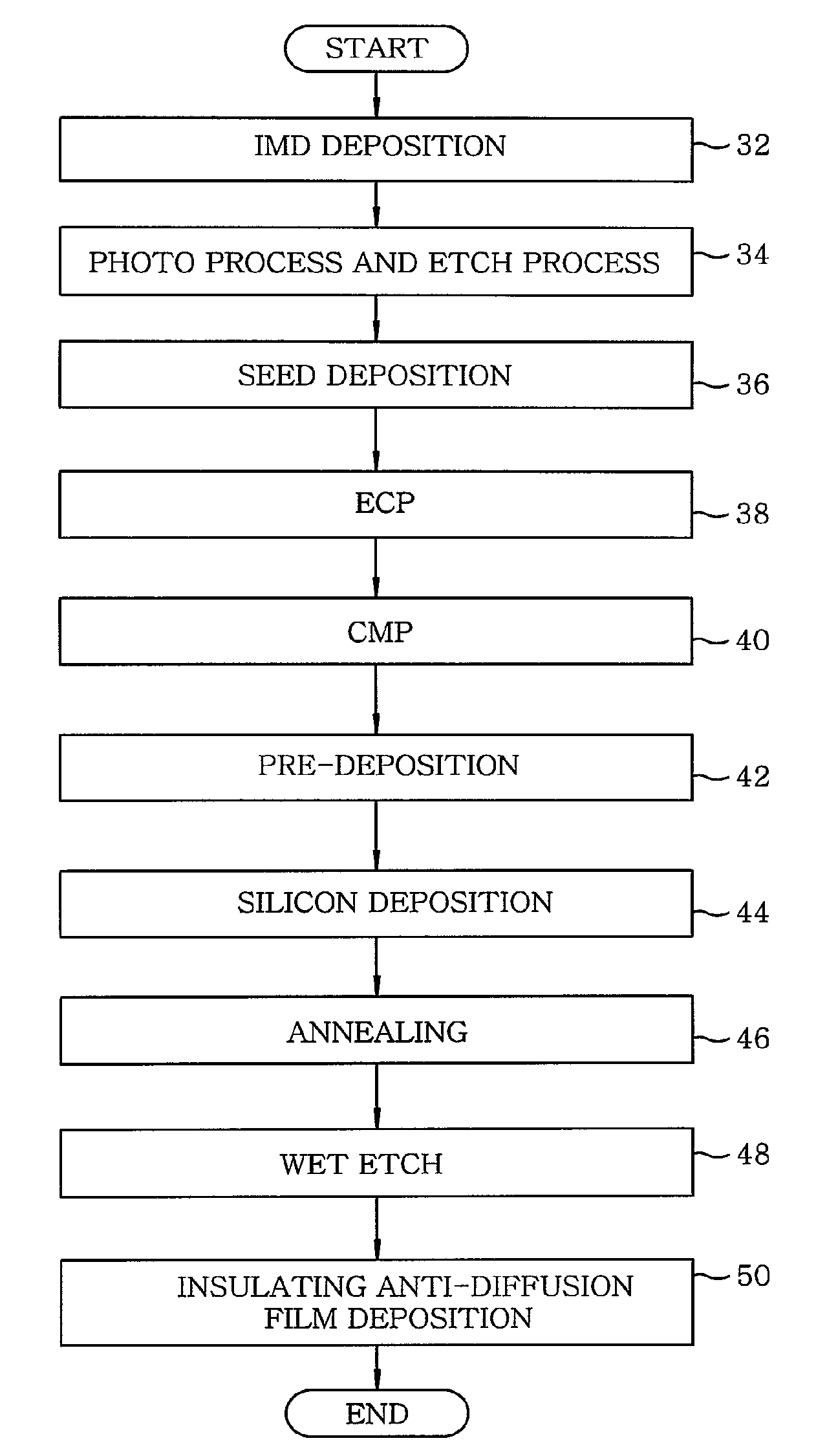
[0038]Referring to FIG. 3, there is shown a process flowchart illustrating a method of forming a copper metal line in a semiconductor device according to the present invention.

[0039]As shown in FIG. 3, a method of forming a copper metal line of a semiconductor device includes the steps of an IMD (interlayer insulating layer) deposition 32, a photo process and an etch process 34, a seed deposition 36, an electro chemical plating (ECP) 38, a chemical mechanical polishing (CMP) 40, a pre-deposition processing 42, a silicon deposition 44, an annealing 46, a wet etch 48, and an insulating anti-diffusion film deposition 50.

[0040]The IMD deposition 32 is a step of depositing an interlayer insulating layer on a semiconductor substrate in which a lower metal line is formed. In more detail, a first i...


PUM

PropertyMeasurementUnit
thicknessaaaaaaaaaa
thicknessaaaaaaaaaa
pressureaaaaaaaaaa

Abstract

A method of forming a copper metal line in a semiconductor device includes depositing an interlayer insulating layer on a semiconductor substrate having a lower metal line, forming a via contact hole and a metal line pattern in the semiconductor substrate, sequentially depositing a barrier metal film and a copper seed layer, forming a copper film on a surface of the semiconductor substrate, removing the copper film and the barrier metal film, other than the portion of a copper metal line to be formed, removing a native oxide film existing on a surface of the copper metal line of the semiconductor substrate, depositing a silicon layer on the semiconductor substrate, making the deposited silicon layer and copper metal react to each other to form a copper silicide layer, removing a remaining silicon layer without being reacted, and depositing an insulating anti-diffusion film over the semiconductor substrate.

Description

FIELD OF THE INVENTION[0001]The present invention relates to semiconductor devices and, more particularly, to a semiconductor having copper metal line and a method of forming the semiconductor capable of preventing the degradation of an electromigration (EM) characteristic caused by poor adhesion and an unstable surface state between the copper metal line and an insulating anti-diffusion film used when forming the copper metal line by a dual damascene method.BACKGROUND OF THE INVENTION[0002]Presently, in order to fabricate semiconductor devices with a fast operating speed and high reliability, a metal of copper is used as a metal line material because it has a low resistivity and high resistance against electrical movement or stress compared with a conventional metal of aluminum (Al).[0003]However, a copper metal line is difficult to be etched by an existing dry etch method. Thus, the copper metal line is generally patterned by a single damascene method or a dual damascene method.[0...

Claims


Application Information

Patent Timeline
Patent Type & Authority Patents(United States)
IPC IPC(8): H01L21/4763
CPCH01L21/76849H01L21/76867H01L21/76886H01L23/53238H01L2924/0002H01L2924/00H01L21/28
Inventor PARK, HYUK
Owner DONGBU HITEK CO LTD
Why Eureka
Try Eureka