Semiconductor integrated test structures for electron beam inspection of semiconductor wafers

a technology of semiconductor wafers and integrated test structures, which is applied in the direction of individual semiconductor device testing, semiconductor/solid-state device testing/measurement, instruments, etc., can solve the problems of increasing inspection time, analysis and cost, and reducing the efficacy of voltage contrast inspection, so as to facilitate the detection of voltage contrast defects

Active Publication Date: 2010-03-16
SAMSUNG ELECTRONICS CO LTD +2
View PDF2 Cites 110 Cited by
  • Summary
  • Abstract
  • Description
  • Claims
  • Application Information

AI Technical Summary

Problems solved by technology

For conductive features, electrical defects can be detected as voltage contrast defects due to charging differences between defective structures and non-defective structures.
This is undesirable for several reasons.
For instance, the need to perform two e-beam scans at different landing energies increases the inspection time and analysis and cost.
Moreover, performing a second scan using a high landing energy beam is problematic in that the high energy electron beam can lead to significant charge accumulation of inspected features, which can cause distortions in an SEM image in way that decreases the efficacy of voltage contrast inspection.
Moreover, the high-levels of accumulated charges that results from high energy electron beam scans can cause damage to certain semiconductor integrated circuit elements, thus lowering yield.

Method used


Image

  • Semiconductor integrated test structures for electron beam inspection of semiconductor wafers
  • Semiconductor integrated test structures for electron beam inspection of semiconductor wafers
  • Semiconductor integrated test structures for electron beam inspection of semiconductor wafers

Examples


Embodiment Construction

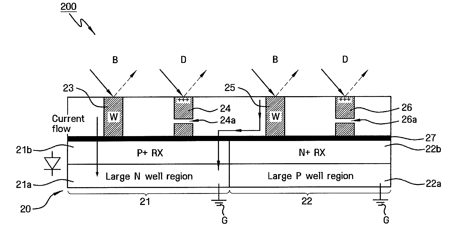
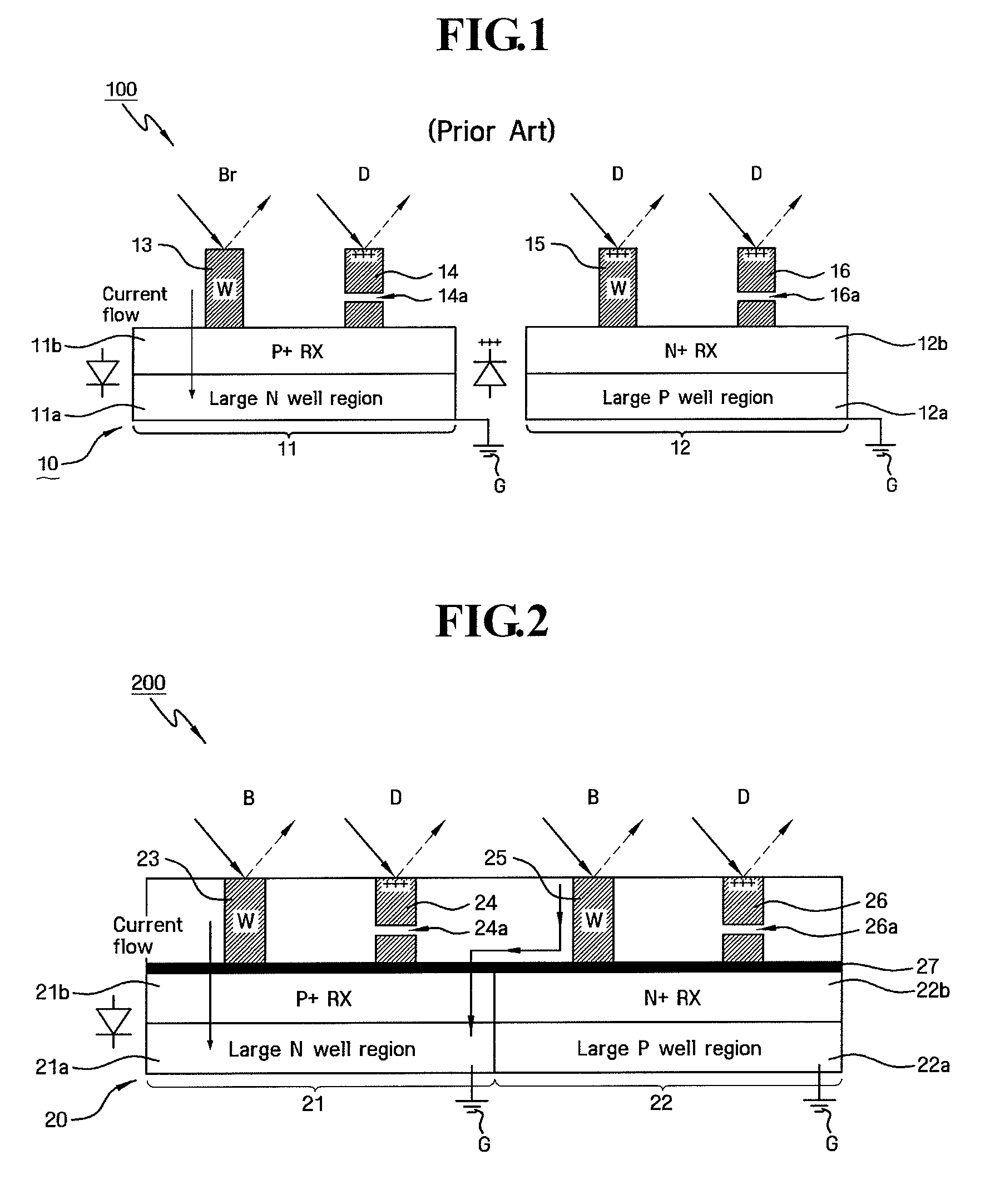
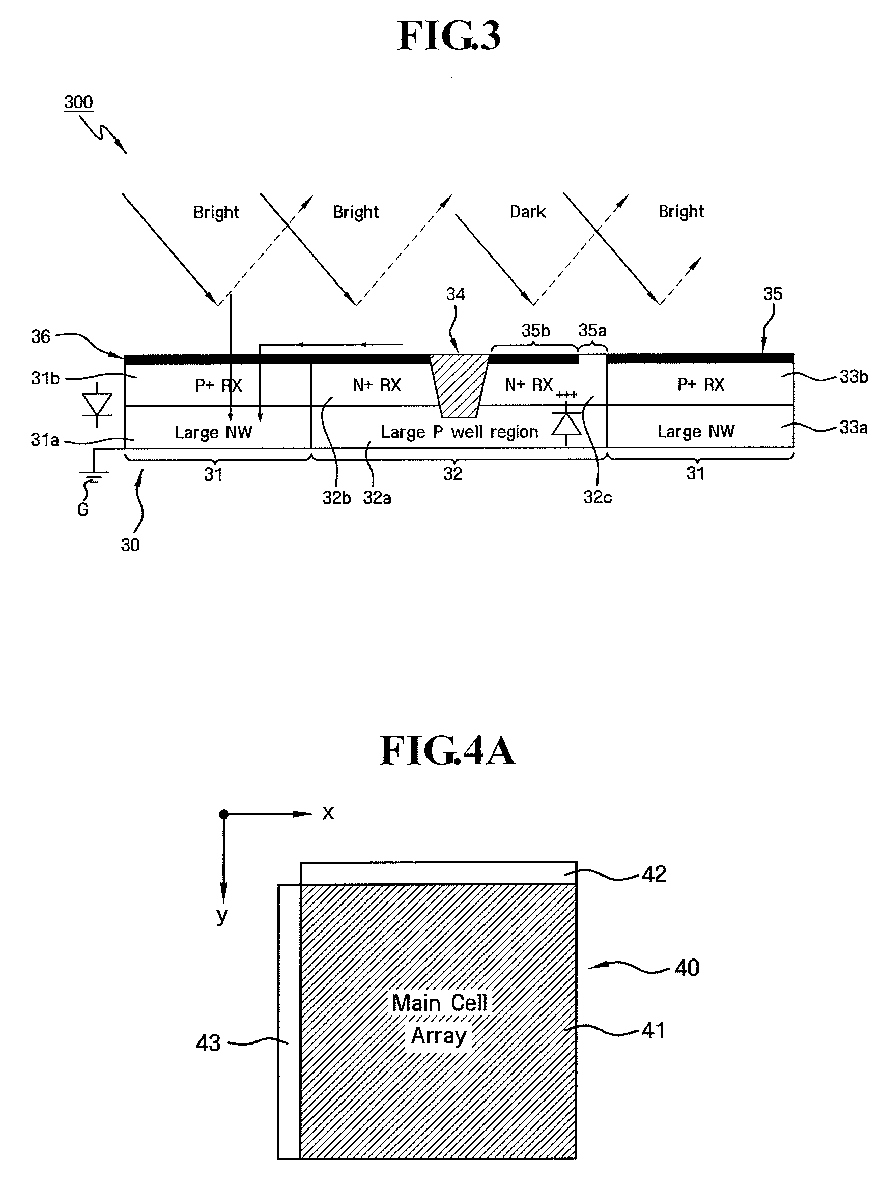
[0032]Exemplary embodiments of semiconductor test structures for use with e-beam contrast inspection to detect electrical defects on semiconductor wafers will now be described more fully with reference to the schematic illustrations of FIGS. 2-7, where it is to be understood that the thickness and dimensions of various structures, layers and regions of semiconductor devices illustrated in the Figures are not to scale but rather exaggerated for clarity. It is to be further understood that when a layer is described as being “on” or “over” another layer or substrate, such layer may be directly on the other layer or substrate, or intervening layers may also be present. Moreover, similar reference numerals used throughout the drawings denote elements having the same or similar functions.

[0033]For illustrative purposes, exemplary embodiments of the invention will be described herein in the context of CMOS integrated circuit fabrication techniques, wherein test structures are designed to a...


PUM


Abstract

Semiconductor integrated test structures are designed for electron beam inspection of semiconductor wafers. The test structures include pattern features that are formed in designated test regions of the wafer concurrently with pattern features of integrated circuits formed on the wafer. The test structures include conductive structures that are designed to enable differential charging between defective and non-defective features (or defective and non-defection portions of a given feature) to facilitate voltage contrast defect detection of CMOS devices, for example, using a single, low energy electron beam scan, notwithstanding the existence of p / n junctions in the wafer substrate or other elements / features.

Description

TECHNICAL FIELD OF THE INVENTION[0001]The present invention relates generally to semiconductor integrated test structures for electron beam inspection of semiconductor wafers and, in particular, semiconductor integrated test structures that are formed in test regions of a semiconductor wafer to detect electrical and physical defects through voltage contrast inspection of the integrated test structures.BACKGROUND[0002]Due to continuing technological innovations in the field of semiconductor fabrication, integrated circuit chips are being developed with larger scale of integration and higher device density, as well as lower power consumption and higher operating speeds. In general, integrated circuits are manufactured using FEOL (front-end-of-line) processing technologies to form discrete semiconductor devices within the surface of a silicon wafer followed by BEOL (back-end-of-line) processing techniques to form a multi-level metallurgical interconnection network over the semiconducto...

Claims


Application Information

Patent Timeline
Patent Type & Authority Patents(United States)
IPC IPC(8): H01L23/58
CPCH01L22/32H01L22/00
Inventor SUN, MIN CHULJANSEN, SCOTTMANN, RANDYPATTERSON, OLIVER D.
Owner SAMSUNG ELECTRONICS CO LTD
Why Eureka
Try Eureka