Supercharge Your Innovation With Domain-Expert AI Agents!

Semiconductor laser device, and image display device

a semiconductor laser and laser technology, applied in semiconductor lasers, instruments, optics, etc., can solve the problems of large electric power consumption, unduly heated semiconductor laser devices, and inability to secure the watt-class high-output performance of semiconductor laser devices, etc., to achieve long operation life and long operation life

Inactive Publication Date: 2010-03-16
PANASONIC CORP
View PDF11 Cites 5 Cited by
  • Summary
  • Abstract
  • Description
  • Claims
  • Application Information

AI Technical Summary

Benefits of technology

"The present invention provides a semiconductor laser device and an image display device that can operate at a low-consumption current and a low-consumption electric power. The semiconductor laser device includes a base block with wirings connected to stripe laser electrodes, which efficiently release heat from the stripe active regions and allow for uniform current supply. The image display device includes laser light sources, such as red, green, and blue laser light sources, which can be operated at a low-consumption current and a low-consumption electric power. The laser light sources can be used in a backlight illuminator for a liquid crystal display panel, providing long operation life. The technical effects of the invention are efficient heat release, low-consumption current, and long operation life of the semiconductor laser device and image display device."

Problems solved by technology

Since a watt-class high-output performance is required to drive the semiconductor laser device, a large electric current supply is required, which results in a large electric power consumption.
As a result of the large electric power consumption, the semiconductor laser device is unduly heated.
As the further heating progresses, it may be impossible to secure the watt-class high-output performance of the semiconductor laser device, or the semiconductor laser device may be degraded.
In driving the multi-stripe semiconductor laser device in the image display device, unless a heat generated in the stripe active regions is rapidly released from the active regions, the laser output may be saturated by the heat, thereby obstructing the high-output performance.
As a result, another drawback such as unduly increase of an operation electric power may occur.
Also, an increased electric current may degrade the semiconductor laser device.
However, there is not disclosed a method for effectively releasing a heat generated in supplying a large electric current to a semiconductor laser device, or a method for uniformly supplying an electric current to stripe active regions.
The third and the fourth conventional arts disclose an approach of directly cooling an emission point of a semiconductor laser element, a laser chip, or a laser bar, but do not disclose an approach of efficiently cooling active regions of a semiconductor laser element.
Further, the third and the fourth conventional arts do not disclose a safety-oriented arrangement of suspending an operation of a semiconductor laser device in the case where the semiconductor laser device is tilted by e.g. tipping over.

Method used


Image

  • Semiconductor laser device, and image display device
  • Semiconductor laser device, and image display device
  • Semiconductor laser device, and image display device

Examples


first embodiment

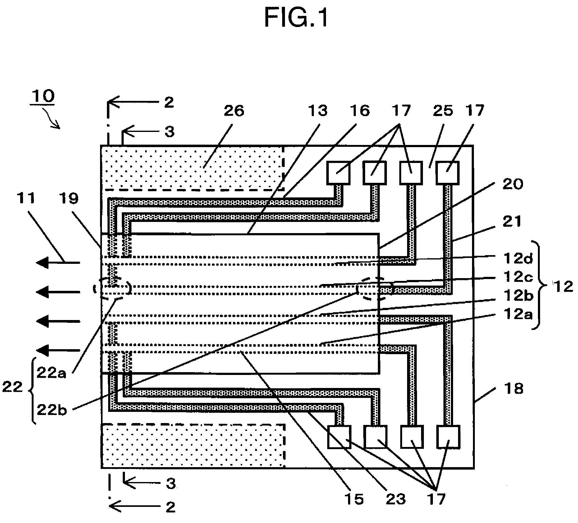
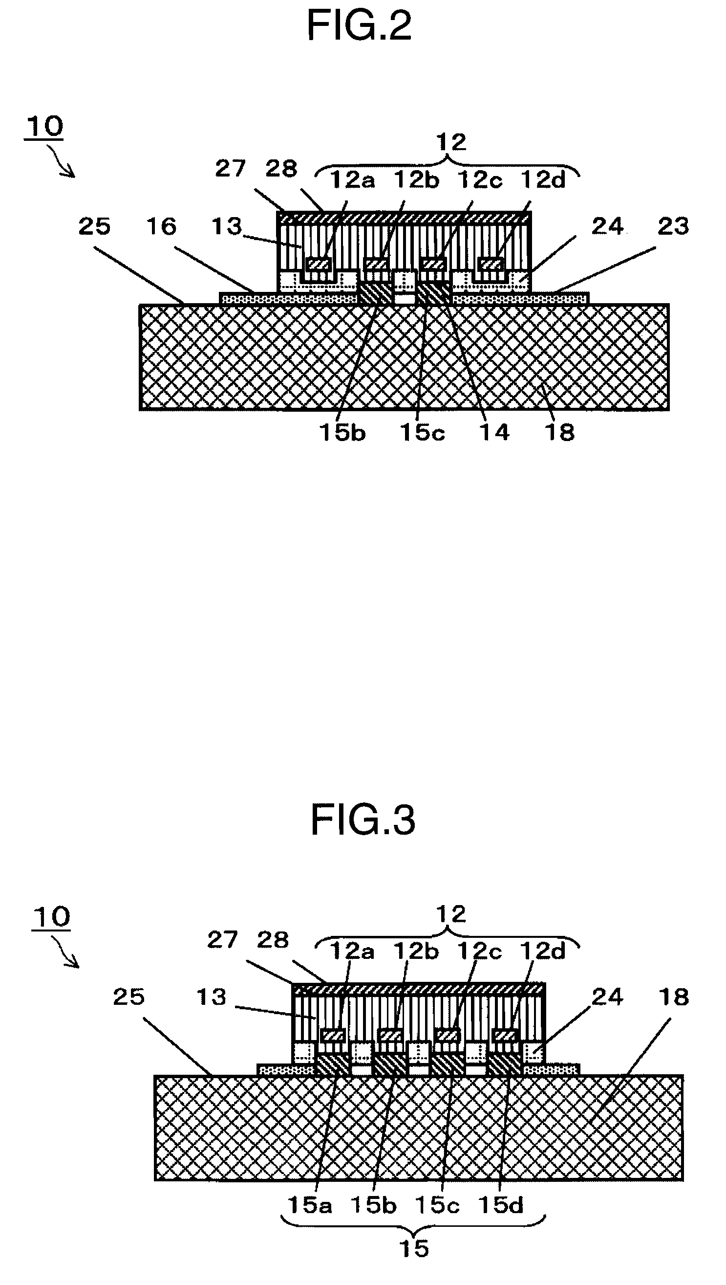
[0054]FIGS. 1 through 4B are diagrams for describing a semiconductor laser device as the first embodiment of the invention. FIGS. 1 through 3 are diagrams schematically showing an arrangement of a semiconductor laser device 10 as the first embodiment of the invention. FIG. 1 is a top plan view schematically showing a mounted state of the semiconductor laser device 10 as the first embodiment. FIG. 2 is a cross-sectional view, taken along the line 2-2 in FIG. 1, schematically showing the mounted state of the semiconductor laser device 10. FIG. 3 is a cross-sectional view, taken along the line 3-3 in FIG. 1, schematically showing the mounted state of the semiconductor laser device 10.

[0055]As shown in FIGS. 1 and 2, the semiconductor laser device 10 includes a semiconductor laser element 13 having multiple stripe active regions 12 i.e. stripe active regions 12a, 12b, 12c, and 12d for emitting laser beams 11; and a base block 18 provided with wirings and electrode parts 17. Stripe laser...

second embodiment

[0068]FIGS. 5 through 9 are diagrams for describing a semiconductor laser device as the second embodiment of the invention. FIGS. 5 through 8 are diagrams schematically showing an arrangement of a semiconductor laser device 30 as the second embodiment. FIG. 5 is a top plan view schematically showing a mounted state of the semiconductor laser device 30 as the second embodiment. FIG. 6 is a cross-sectional view, taken along the line 6-6 in FIG. 5, schematically showing the mounted state of the semiconductor laser device 30. FIG. 7 is a cross-sectional view, taken along the line 7-7 in FIG. 5, schematically showing the mounted state of the semiconductor laser device 30. FIG. 8 is across-sectional view, taken along the line 8-8 in FIG. 5, schematically showing the mounted state of the semiconductor laser device 30.

[0069]As shown in FIGS. 5 and 6, the semiconductor laser device 30 includes a semiconductor laser element 13 having multiple stripe active regions 12 i.e. stripe active region...

third embodiment

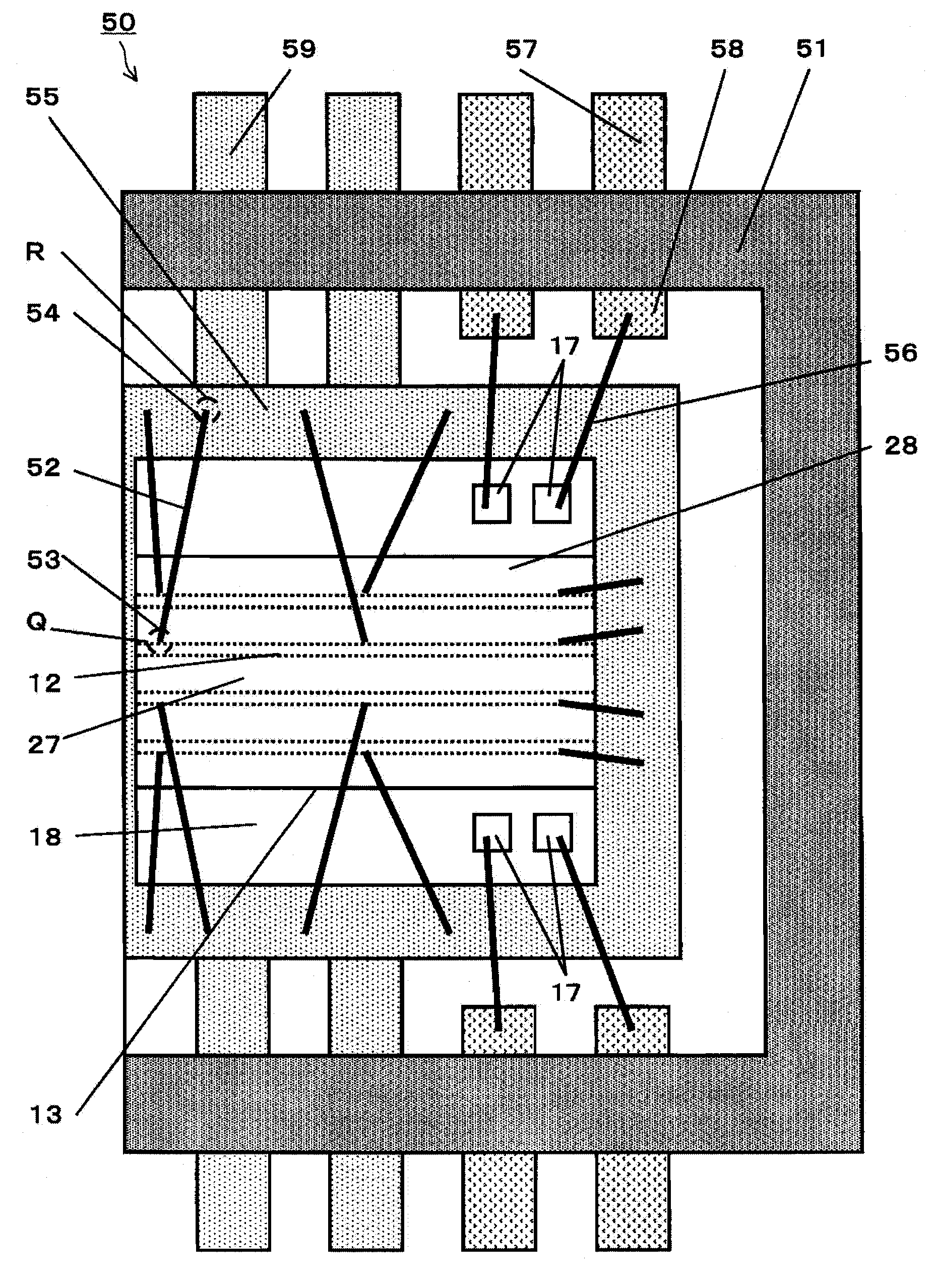
[0078]FIGS. 11 through 14 are diagrams for describing a semiconductor laser device as the third embodiment of the invention. FIG. 11 is a top plan view schematically showing a mounted state of a semiconductor laser device 50 as the third embodiment of the invention. The semiconductor laser device 50 shown in FIG. 11 is constructed by mounting the semiconductor laser device 10 or 30 of the first or the second embodiment in a package 51.

[0079]Specifically, unlike the semiconductor laser device 10 or 30 of the first or the second embodiment, the semiconductor laser device 50 shown in FIG. 11 additionally includes the package 51 for mounting a base block 18 provided with a semiconductor laser element 13. A rear electrode 28 is formed on a second surface 27 of the semiconductor laser element 13, which is opposed to a first surface (not shown) of the semiconductor laser element 13 and in parallel thereto, close to active regions of the semiconductor laser element 13. The rear electrode 28...


PUM


Abstract

A semiconductor laser device and an image display device that efficiently release a heat from stripe active regions, and operated at a low-consumption current and a low-consumption electric power. A semiconductor laser element includes stripe active regions for emitting laser beams. On a base block, there are formed wirings electrically connected to stripe laser electrodes of the semiconductor laser element, respectively. The stripe laser electrodes corresponding to the stripe active regions are formed in proximity to a first surface of the semiconductor laser element, close to the active regions. An electric current is supplied to the active regions from connecting portions between each of the laser electrodes and the wirings.

Description

BACKGROUND OF THE INVENTION[0001]1. Field of the Invention[0002]The present invention relates to a high-performance semiconductor laser device for use in an image display device such as a laser display device, and an image display device incorporated with the semiconductor laser device.[0003]2. Description of the Background Art[0004]In recent years, a large-screened and thin flat panel display device, as represented by plasma display devices or liquid crystal display devices, has been rapidly spread. A laser display device is being developed, as an example of a thin flat panel display device having a larger screen and a larger luminance. A semiconductor laser device with high luminance output and operable at a low-consumption electric power is used as a light source of the laser display device.[0005]Watt-class high-output performance is required for the semiconductor laser device. In view of this, there is used a so-called multi-stripe semiconductor laser element constructed in such...

Claims


Application Information

Patent Timeline
Patent Type & Authority Patents(United States)
IPC IPC(8): H01S5/00
CPCH01S5/4031H04N9/3129G02F1/133621H01S5/005H01S5/02232H01S5/0224H01S5/02272H01S5/02276H01S5/02423H01L2224/48247H01L2224/49171H01S5/0234H01S5/0237H01S5/02345
Inventor YAMAMOTO, KAZUHISAMIZUUCHI, KIMINORIKADOWAKI, SHINICHI
Owner PANASONIC CORP
Features
  • R&D
  • Intellectual Property
  • Life Sciences
  • Materials
  • Tech Scout
  • Unparalleled Data Quality
  • Higher Quality Content
  • 60% Fewer Hallucinations
Learn More