Synchronous type semiconductor device for high speed data processing

a semiconductor device and data processing technology, applied in the field of synchronous semiconductor devices, can solve the problems of reducing the operating margin when operating at a high frequency, and achieve the effects of preventing erroneous information samples, stable operation, and reducing the pulse width of each internal clock signal

Active Publication Date: 2010-03-16
MICRON TECH INC
View PDF5 Cites 5 Cited by
  • Summary
  • Abstract
  • Description
  • Claims
  • Application Information

AI Technical Summary

Benefits of technology

[0016]Accordingly, an object of the present invention is to provide a synchronous type semiconductor device that secures a margin for preventing erroneous sampling of information in an immediately preceding cycle or a margin for reducing the pulse width of each internal clock signal even in a high-frequency operation.
[0066]According to the present invention, even in a high-frequency operation, a margin for preventing erroneous sample of information in an immediately preceding cycle or a margin for reducing a pulse width of each internal clock signal can be secured. A stable operation can be thus implemented.

Problems solved by technology

The configuration shown in FIG. 1, however, may cause a reduction in an operating margin when operated at a high frequency.

Method used


Image

  • Synchronous type semiconductor device for high speed data processing
  • Synchronous type semiconductor device for high speed data processing
  • Synchronous type semiconductor device for high speed data processing

Examples


first embodiment

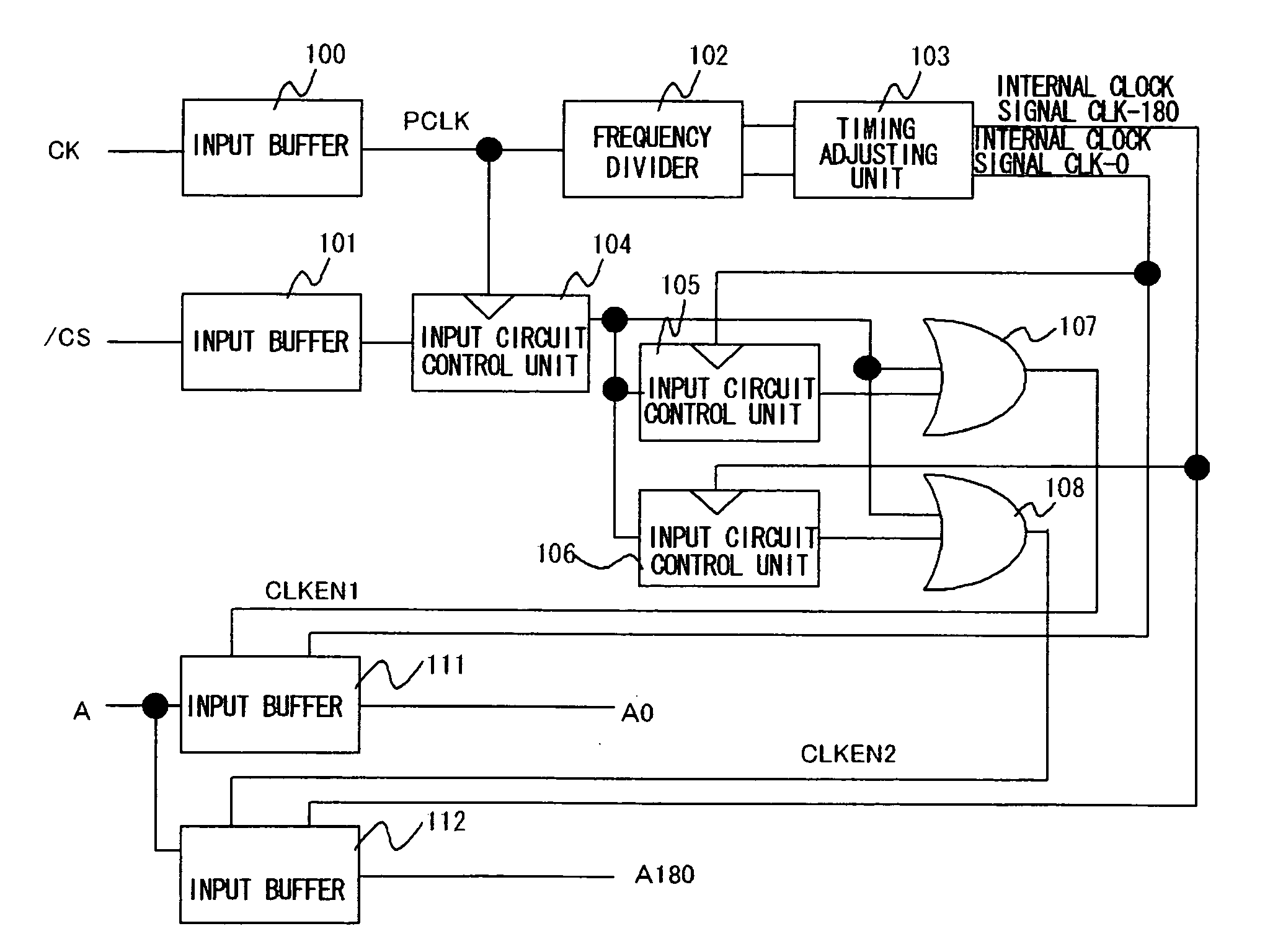
[0075]FIG. 3 is a diagram showing a configuration of a synchronous type semiconductor device according to the present invention, and corresponds to a configuration (an input portion of a synchronous DRAM) in FIG. 1. The input buffer 100, frequency divider 102, and timing adjusting unit 103 constitute a clock generation circuit. The timing adjusting unit 103 includes delay circuit or the like. The input buffer 100 receives the external clock signal CK. The frequency divider 102 frequency divides an output of the input buffer 100. The timing adjusting unit 103 receives an output of the frequency divider 102 and generates the two-phase internal clock signals CLK-0 and CLK-180.

[0076]The input buffer 101 receives the chip select signal / CS. The input buffer 101, input circuit control units 104, 105 and 106, and OR circuits 107 and 108 constitute a chip select circuit.

[0077]The input circuit control unit 104 latches and outputs the chip select signal output from the input buffer 101 respo...

second embodiment

[0089]Next, another embodiment of the present invention will be described. FIG. 5 is a diagram showing an overall configuration of a synchronous type semiconductor device according to the present invention.

[0090]This embodiment includes the input buffer 100, frequency divider 102, timing adjusting unit 103, input buffer 101, input circuit control unit 109, input circuit control unit 110, input circuit control unit 105, input circuit control unit 106, OR circuit 107, and OR circuit 108. The input buffer 100 receives the external clock signal CK. The frequency divider 102 frequency divides the clock signal (PCLK) output from the input buffer 100, thereby outputting the first frequency-divided clock signal DIVCLK1 and the second frequency-divided clock signal DIVCLK2 having different phases. The timing adjusting unit 103 receives the first frequency-divided clock signal DIVCLK1 and the second frequency-divided clock signal DIVCLK2 from the frequency divider 102 and generates the two-ph...


PUM


Abstract

Disclosed is a synchronous semiconductor device including clock generation circuit that frequency divides a clock signal (PCLK) input from an input buffer and generates first and second internal clock signals having a predetermined phase difference from first and second frequency-divided clock signals of different phases, respectively, a first input circuit control unit that receives a chip select signal and samples the chip select signal in synchronization with the clock signal, second and third input circuit control units that sample an output of the first input circuit control unit in synchronization with the first and second internal clock signals, respectively, and first and second input circuits that receive a result of a logic operation between the output of the first input control unit and an output of the second input circuit control unit and a result of a logic operation between the output of the first input circuit control unit and an output of the third input circuit control unit as input enable signals, respectively, and sample an externally input signal in synchronization with the first and second internal clock signals, respectively based on enabling instructed by the input enable signals.

Description

FIELD OF THE INVENTION[0001]The present invention relates to a semiconductor device. More specifically, the invention relates to a synchronous semiconductor device adapted to reduce power consumption of an input circuit therein.BACKGROUND OF THE INVENTION[0002]As one of techniques for reducing power consumption, using a potential level state of a chip select signal / CS (in which a symbol / before a signal name CS indicates active low), control is performed so that when a potential level of a signal CSB (which is an inverted signal of the signal CS) is HIGH,[0003]two-phase internal clocks to be supplied to a command, address, and data input system are stopped,[0004]a synchronous type input buffer is stopped, or[0005]a latch circuit portion of an asynchronous type buffer, which uses a flip-flop circuit or the like, is stopped (such that an output signal of a latch circuit does not transition).[0006]In a synchronous DRAM in particular, only when the chip select signal / CS is LOW, a comma...

Claims


Application Information

Patent Timeline
Patent Type & Authority Patents(United States)
IPC IPC(8): G06F1/12
CPCG06F1/06
Inventor KUROKI, KOJI
Owner MICRON TECH INC
Why Eureka
Try Eureka