Signal integrity measurement systems and methods using a predominantly digital time-base generator

a technology of time-base generator and signal integrity measurement, which is applied in the direction of noise figure or signal-to-noise ratio measurement, instruments, recording signal processing, etc., can solve the problems of circuit failure, current level, analog transients in voltage level,

Inactive Publication Date: 2010-03-16
DFT MICROSYST
View PDF72 Cites 19 Cited by
  • Summary
  • Abstract
  • Description
  • Claims
  • Application Information

AI Technical Summary

Problems solved by technology

Consequently, when digital signals transition inside or outside a semiconductor device, they cause analog transients in voltage level, current level, or both.
For example, if the time it takes for a voltage to transition from a “0”-level to a “1”-level is excessively long, the semiconductor device may cease to operate altogether.
Similarly, if a logical “1” (“0”) is encoded using too low (high) a voltage or current, the resulting circuit could fail to operate correctly.
If the timing of the digital signals from the source to the destination is excessively perturbed, the resulting communication link could be corrupted.
However, entire systems are currently being constructed onto a very small form factor.
The current-generation test and measurement technology is not capable of analyzing internal circuitry because of access difficulties.
To test is to disturb, so transferring a very low level signal from the micro-scale of a modern device to the macro scale of the test instrument is too disruptive to the signal being measured.
In general, the clocking circuit is the most important and most challenging component in an instrument such as an oscilloscope or a jitter analyzer in terms of design and implementation.
Much of the clocking challenges occur when the signal frequency is faster than half of the clocking circuit frequency.
Unfortunately, most measurement applications fall into this category.
Such implementation is extremely costly, requires rather large implementation area, and involves significant calibration procedures.
These limitations make this technology generally suitable only for single-channel high-end equipment such as wide-bandwidth oscilloscopes.
For obvious reasons it is not suited for integration as a signal-integrity measurement macro within a semiconductor device.
Both methods described above have serious limitations associated with the reliable generation of small delay increments and with accumulated jitter in any circuitry that generates such delay increments.
The impact of unwanted jitter on A / D-converter performance can be severe, and in the case of test and measurement applications, jitter is often the very phenomenon being measured.
This concept is referred to as a “vernier delay line.” Apart from the obvious increase in implementation area, it is extremely difficult to match the delay values of both vernier delay lines.
For some applications such as built-in test, such as disclosed in U.S. Pat. No. 7,158,899, these elaborate schemes cannot be employed, thus rendering the performance of the resulting solution very questionable.
Controlling the wander or filtering it out in a post-processing step is extremely challenging.

Method used


Image

  • Signal integrity measurement systems and methods using a predominantly digital time-base generator
  • Signal integrity measurement systems and methods using a predominantly digital time-base generator
  • Signal integrity measurement systems and methods using a predominantly digital time-base generator

Examples


Embodiment Construction

1.0 Overview

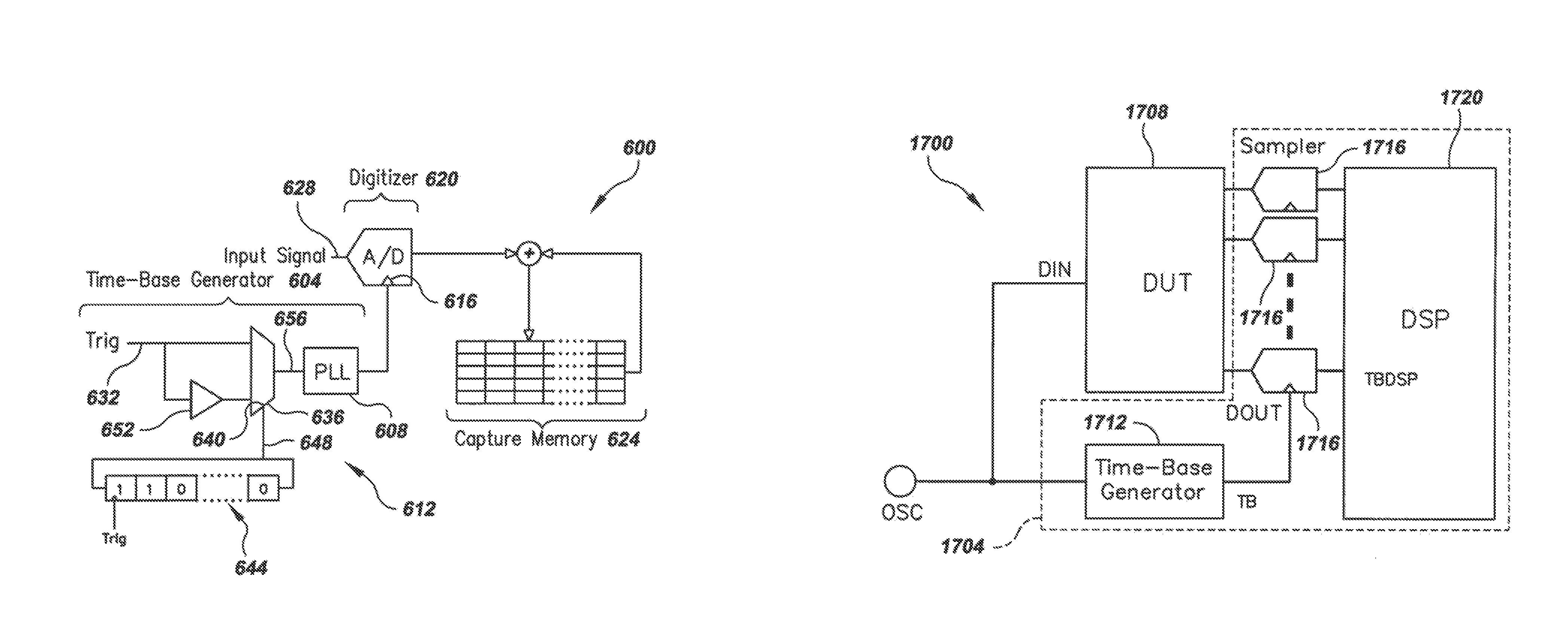
[0039]For the purposes of various embodiments of signal-integrity measurement systems and methods of present invention, unique time-base generation techniques are utilized that can achieve 100 fsec sampling resolution, or less, while deploying extremely simple hardware. As described below, signal-integrity measurement solutions disclosed herein are free of various limitations that plague conventional testing systems, such as delay line non-linearity, area overhead, jitter, and even wander between offset frequency oscillators. Instead, the disclosed time-based generation techniques offer deterministic sampling instants at an extremely fine resolution. Fine resolution is defined here as any delay resolution that is less than the minimum attainable using conventional delay lines. These time-base generation techniques may be implemented in conjunction with various samplers and various digital signal collecting and processing techniques to enable extremely efficient signal-in...


PUM


Abstract

Signal-integrity measurement systems and methods utilizing unique time-base generation techniques for controlling the sampling of one or more signals under test. A time-base generator made in accordance with the present disclosure includes a phase filter and modulation circuitry that generates a rapidly varying phase signal as a function of the output of a sigma-delta modulator. The phase filter filters unwanted high-frequency phase components from the rapidly varying phase signal. The filtered signal is used to clock one or more samplers so as to create sampling instances of the signal(s) under test. The sampling instances are then analyze using any one or more of a variety of techniques suited to the type of signal(s) under test.

Description

RELATED APPLICATION DATA[0001]This application claims the benefit of priority of U.S. Provisional Patent Application Ser. No. 60 / 830,797, filed on Jul. 14, 2006, and titled “Signal Integrity Measurement System And Method Using A Predominantly Digital Time-Base Generator,” which is incorporated herein by reference in its entirety.FIELD OF INVENTION[0002]The present invention relates generally to signal integrity measurement of digital circuits and systems. More particularly, the present invention is directed to signal integrity measurement systems and methods of using a predominantly digital time-base generator.BACKGROUND[0003]While digital circuits are ultimately intended to process discrete values—such as “0” and “1,” at the semiconductor device level, such circuits invariably encode discrete signals using physical quantities such as voltage and current. Consequently, when digital signals transition inside or outside a semiconductor device, they cause analog transients in voltage l...

Claims


Application Information

Patent Timeline
Patent Type & Authority Patents(United States)
IPC IPC(8): G06K5/04G06F11/00G06K5/00G01M99/00
CPCG01R31/2882G01R31/31709G01R31/31725G01R31/31727
Inventor HAFED, MOHAMED M.
Owner DFT MICROSYST
Why Eureka
Try Eureka