Bonding method for through-silicon-via based 3D wafer stacking

a technology of throughsilicon and via, applied in the direction of electrical equipment, semiconductor devices, semiconductor/solid-state device details, etc., can solve the problems of inferior electrical connection at the via, difficulty in implementing the method, and high bonding temperatur

Active Publication Date: 2010-03-23
HONG KONG APPLIED SCI & TECH RES INST
View PDF21 Cites 86 Cited by
  • Summary
  • Abstract
  • Description
  • Claims
  • Application Information

AI Technical Summary

Problems solved by technology

Diffusion bonding produces a good quality bond that is reliable, but disadvantages of this method include the requirements for very good coplanarity of the two semiconductor components and the need for a high bonding temperature.
The method is therefore difficult to implement and is expensive.
However, while adhesive bonding is low cost and does not present significant manufacturing problems, it provides inferior electrical connections at the vias and is not generally suitable for high current use and is unreliable.
However, soldering encounters problems as the number of components being stacked increases.
In such methods, however, when a new wafer is added to a stack and a soldering process is carried out to form an IMC connecting the new wafer to the stack, the previously formed IMCs between other wafers grow very fast under the high soldering temperature.
Since the IMC is usually a hard and brittle material so as it grows failure issues will occur (e.g., in the drop qualification test).
Furthermore, if the volume of the solder materials is not controlled well in the manufacturing process, in multiple solder bonding steps the remained solders, which are not formed IMCs, will be reflowed again, this will undermine their reliability and generate manufacturing defects, leading to potential failures in severe conditions.

Method used


Image

  • Bonding method for through-silicon-via based 3D wafer stacking
  • Bonding method for through-silicon-via based 3D wafer stacking
  • Bonding method for through-silicon-via based 3D wafer stacking

Examples


Embodiment Construction

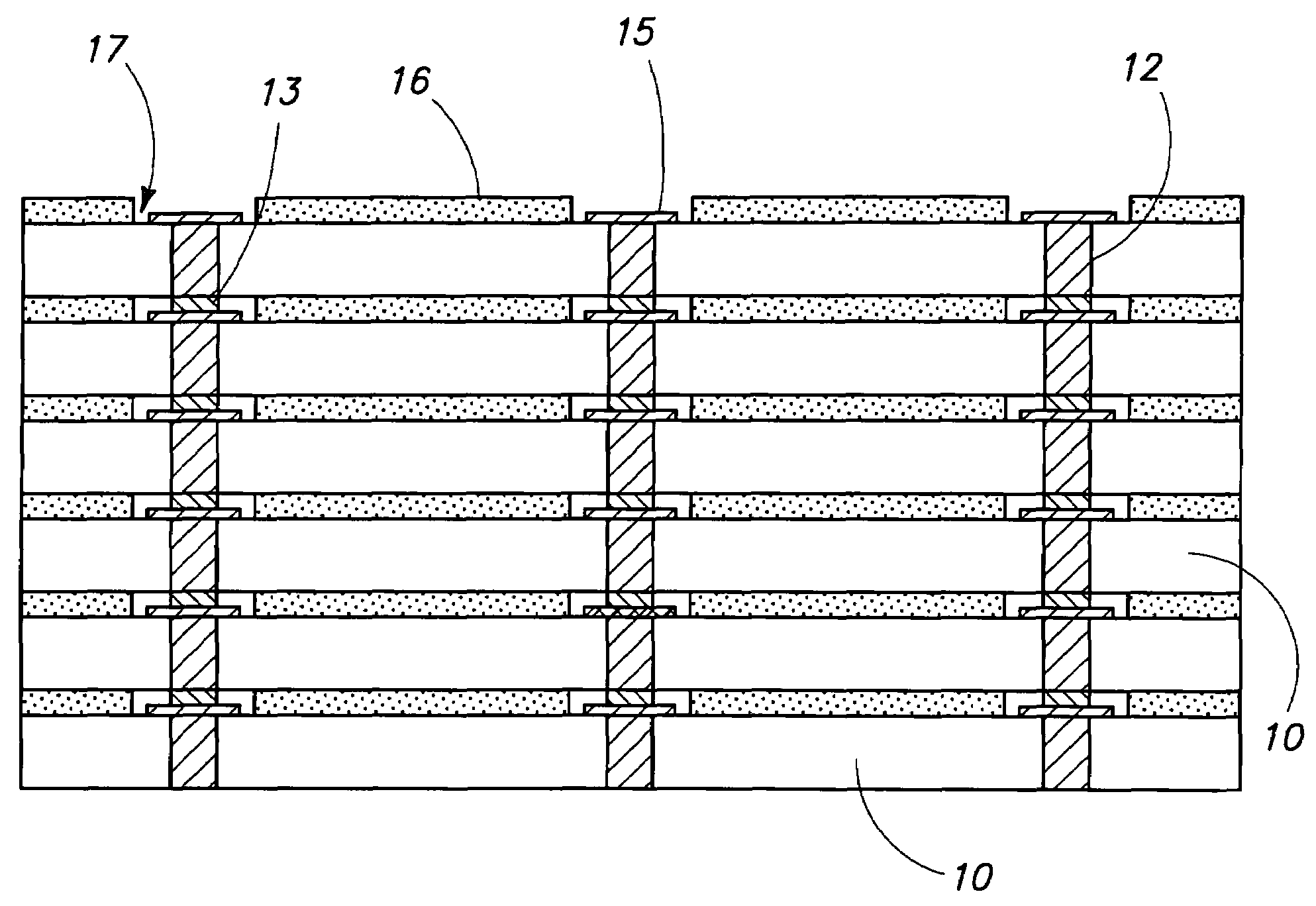
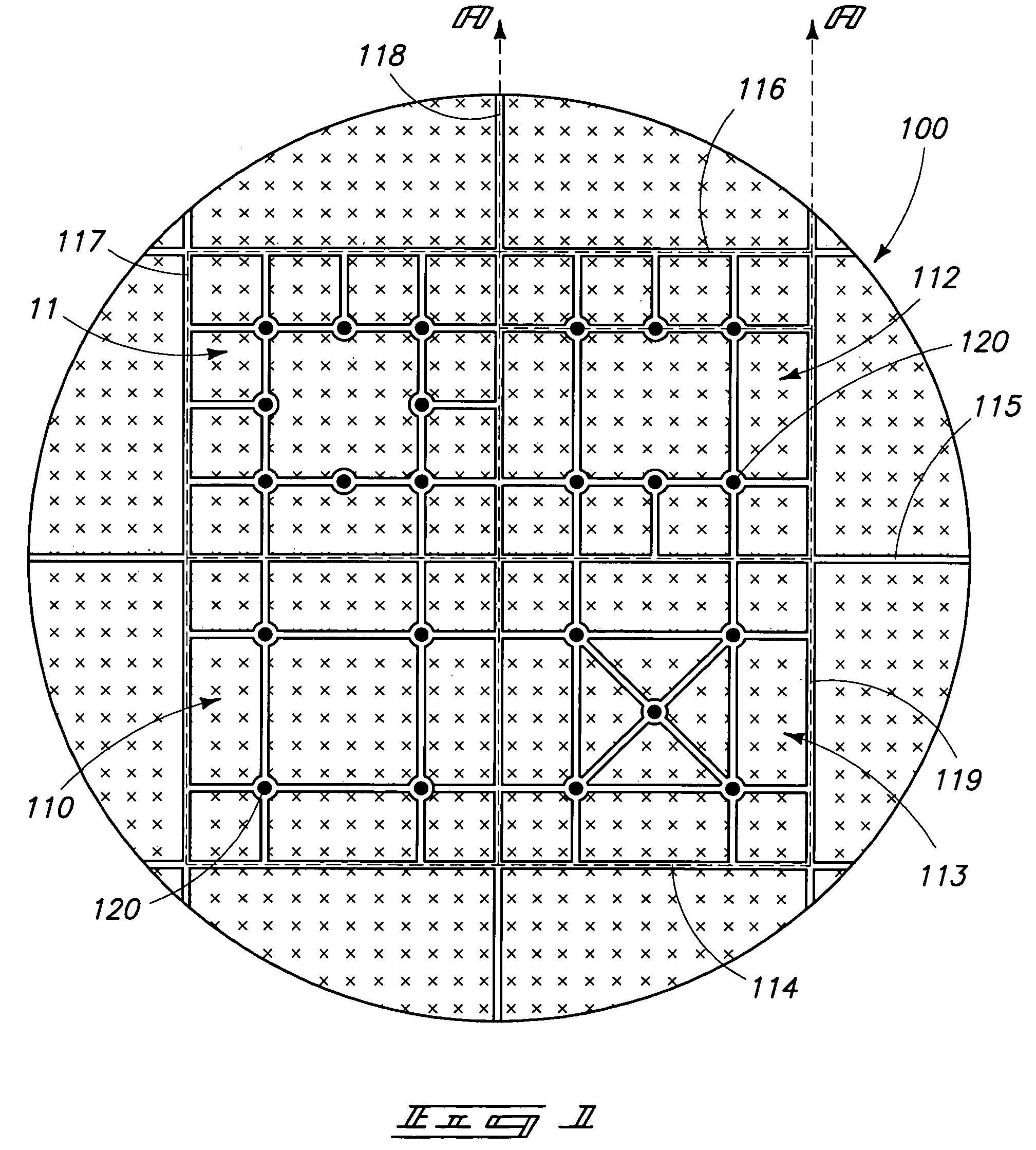
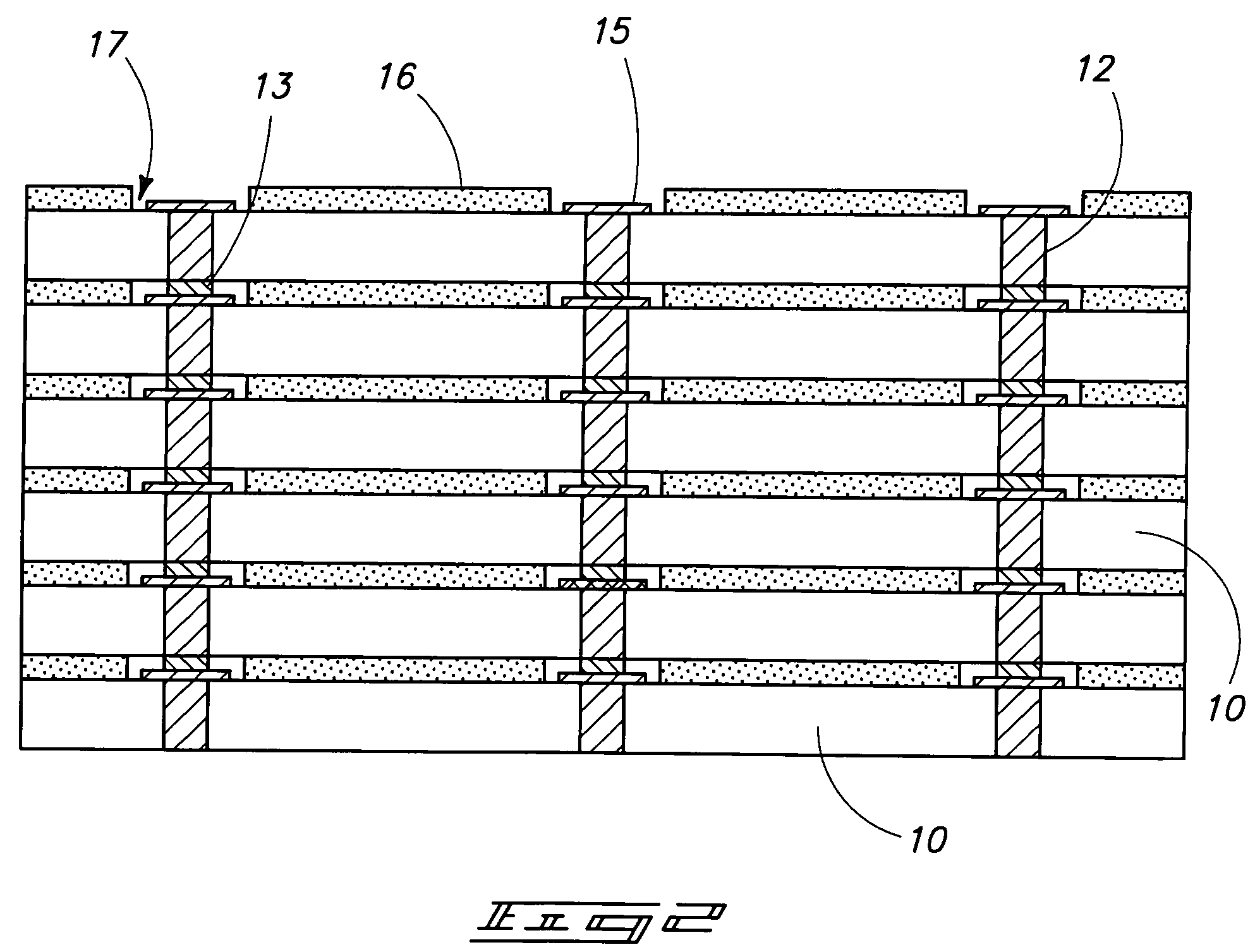
[0022]FIG. 1 shows an embodiment of the invention in the form of a circular wafer stack 100 which may be divided into four chips 110-113. FIG. 2 is a cross-sectional view along line A-A showing the structure of the wafer stack with a plurality of TSVs electrically connected by solder and with individual wafers bonded together by layers of adhesive that are patterned in a manner to be described below.

[0023]In this example each chip 110-113 has a different arrangement of vias 120 (e.g., a simple square in 110, two rows of three vias in 11 and 112, and a square with a central via in chip 113), but in each case every via is formed with a surrounding space that connects to an edge of the chip through channels either directly or through another surrounding space. It will be seen that the four chips are divided by mutually perpendicular main rows 114-119 that are channels formed by patterning the adhesive and which lead to the edge of the wafer. Each channel in one of the chips 110-113 ult...


PUM


Abstract

There is described a hybrid bonding method for through-silicon-via based wafer stacking. Patterned adhesive layers are provided to join together adjacent wafers in the stack, while solder bonding is used to electrically connect the vias. The adhesive layers are patterned to enable outgassing and to provide stress relief.

Description

FIELD OF THE INVENTION[0001]This invention relates to a bonding method for through-silicon-via based 3D wafer stacking, in particular the invention relates to a hybrid bonding method employing aspects of both adhesive and solder bonding. The invention also extends to the resulting wafer stack assembly.BACKGROUND OF THE INVENTION[0002]With electronic devices, particularly portable devices such as mobile phones, becoming smaller and yet at the same time offering a wider range of functions, there is a need to integrate multifunctional chips but without increasing the size of the devices and keeping a small form factor. Increasing the number of electronic components in a 2D structure is incompatible with these objectives, and therefore 3D packages are increasingly being adopted in order to provide greater functionality and higher component density but with a small form factor.[0003]In a 3D structure electronic components such as semiconductor chips with different active IC devices may b...

Claims


Application Information

Patent Timeline
Patent Type & Authority Patents(United States)
IPC IPC(8): H01L29/40H01L21/00
CPCH01L23/481H01L24/16H01L24/94H01L25/0657H01L25/50H01L24/13H01L2924/0002H01L2224/0401H01L2924/07811H01L2924/10253H01L2924/01074H01L2924/01033H01L21/6836H01L2924/14H01L2924/01327H01L2924/01082H01L24/29H01L24/32H01L24/81H01L24/83H01L2221/6834H01L2224/0557H01L2224/13025H01L2224/13099H01L2224/83194H01L2224/9202H01L2224/9205H01L2224/9212H01L2224/94H01L2225/06541H01L2924/01022H01L2924/01029H01L2924/01046H01L2924/01047H01L2924/01049H01L2924/01078H01L2924/01079H01L2224/83H01L2224/81H01L2924/00H01L2224/05552
Inventor MA, WEISHU, XUNQINGCHUNG, CHANG HWA
Owner HONG KONG APPLIED SCI & TECH RES INST
Why Eureka
Try Eureka