LED chip array module

a chip array module and chip technology, applied in the direction of electrical equipment, semiconductor devices, semiconductor/solid-state device details, etc., can solve the problems of poor reliability, difficult interconnection between chips, and low lumen output per device, so as to achieve easy wiring and reliable electrical connections.

Active Publication Date: 2010-03-23
DICON FIBEROPTICS
View PDF6 Cites 9 Cited by
  • Summary
  • Abstract
  • Description
  • Claims
  • Application Information

AI Technical Summary

Benefits of technology

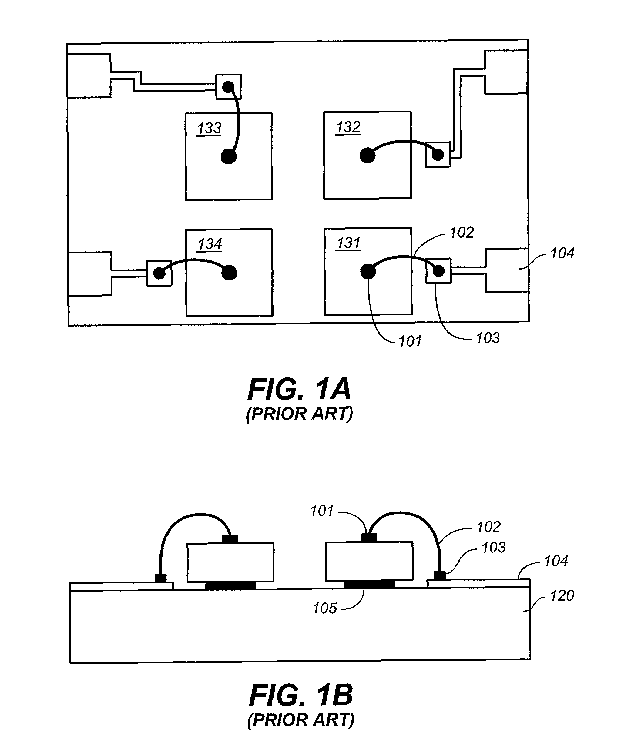
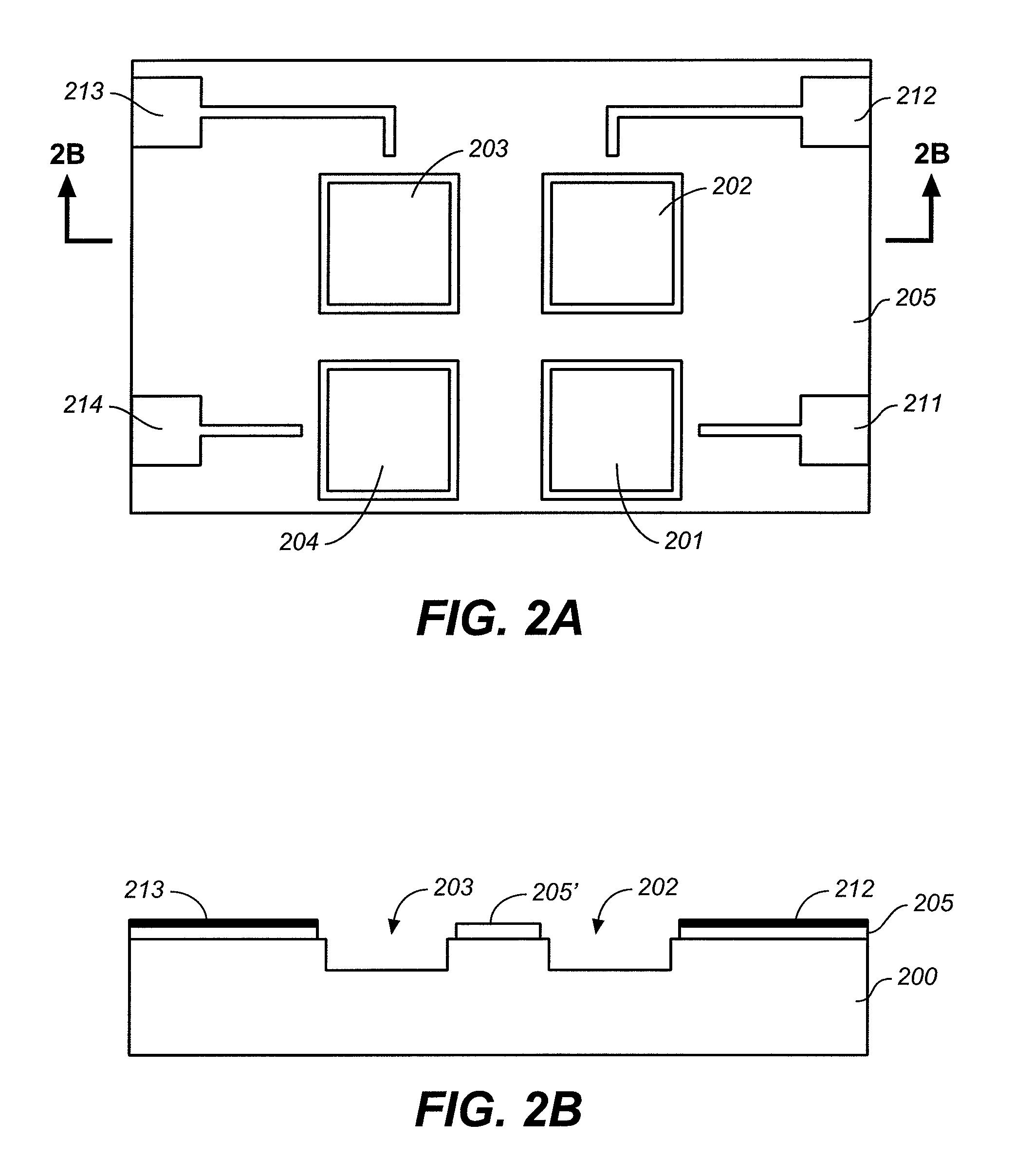
[0003]The above difficulties encountered in conventional LED multiple chip modules can be overcome by using an interconnect to connect the chips to electrodes in a module where the interconnect is supported at points along its length other than at endpoints thereof, by a carrier either directly or indirectly. This improves reliability of the interconnect over conventional designs. Preferably, the contacts of the chips, and the electrodes are all within, or do not extend beyond, two parallel planes that are 400 microns apart. This results in a much more compact module than conventional designs. While preferably the entire length of the interconnect is supported by the carrier, the electrodes or the chip contacts, this is not required, so that it is possible for portions of the interconnect not to be so supported. As long as parts of the interconnect are so supported, reliability of the electrical connections will be much improved over conventional designs, where each bonding wire is supported only at its two ends.
[0006]By using the above described interconnecting structures, use of bond wires is avoided, so that the module is much easier to make, and the electrical connections are more reliable than conventional ones. Techniques used in semiconductor processing may be used in making the interconnect.

Problems solved by technology

The current disadvantages of LEDs compared to conventional light sources are their much higher cost and lower lumen output per device.
As the number of chips in an array increases, interconnections among chips become very difficult and suffer from reliability.
However, limited space for wiring and wire protrusion are a big challenge.

Method used


Image

  • LED chip array module
  • LED chip array module
  • LED chip array module

Examples


Embodiment Construction

[0038]Since their inception in the early 1960's, light emitting diodes have gained widespread use and now can be found nearly everywhere. The devices are fabricated by depositing a stack of epitaxial layers onto a substrate. Normally the deposition starts from electron-excessive layers called n-doped layers, then Multiple Quantum Wells (MQWs) and at last the p-doped layers having holes. When a potential is applied across the device, the electrons and holes move in the opposite directions and combine in the MQWs. This causes light to be emitted with a wavelength and color determined by the energy released when the electrons and holes combine.

[0039]FIGS. 10A and 10C illustrate conventional LED dies (or chips) for GaAs-based (color ranging from red to yellow) and GaN-based (color ranging from green to blue) LED devices, respectively. Epitaxial layers are grown onto a wafer of GaAs, SiC or sapphire. GaAs or SiC are electrically conductive and therefore their arrangement of electrode is ...


PUM


Abstract

The difficulties encountered in conventional LED multiple chip modules where wire bonding is used to connect the chips to electrodes can be overcome by using an interconnect to connect the chip to electrodes in a module where the interconnect is supported at points along its length other than at endpoints thereof, by a carrier either directly or indirectly. This improves reliability of the interconnect over conventional designs. Preferably, the contacts of the chips, and the electrodes are all within, or do not extend beyond, two parallel planes that are 400 microns apart for a compact design.

Description

BACKGROUND OF THE INVENTION[0001]Rapid advances in high-brightness (HB) Light Emitting Diode (LED) technology in the last 10 years have opened up the possibility of using HB-LEDs as sources of general illumination. From 1995 through 2004, the HB-LED exhibited a remarkable growth history, with an average annual growth rate of 46% to a market size of $3.7 billion in 2004. Remarkable progress of LED in external quantum efficiency, lumen output and long lifetime has initiated a market in niche lighting applications. It is believed that LEDs can have a significant share of the general lighting market in the next 10 years.[0002]The current disadvantages of LEDs compared to conventional light sources are their much higher cost and lower lumen output per device. For increasing lumen output, high-density assembly of multiple chips in a compact module is becoming the trend. In a multi-chip assembly, the output color can also be changed dynamically as needed. As the number of chips in an array...

Claims


Application Information

Patent Timeline
Patent Type & Authority Patents(United States)
IPC IPC(8): H01L23/34
CPCH01L25/0753H01L33/483H01L33/62H01L2224/48091H01L2924/00014H01L2224/73265H01L2924/00
Inventor LEE, HO-SHANGLU, JUN-YING
Owner DICON FIBEROPTICS
Why Eureka
Try Eureka