

High-frequency probe card and transmission line for high-frequency probe card
a high-frequency probe and transmission line technology, applied in the field can solve the problems of increasing the difficulty level of critical installation density of the jumping connection structure of transmission lines, and complicating the module engineering of jumping transmission lines, so as to improve the test quality of high-frequency probe cards, reduce the installation density, and simplify the effect of module engineering of setting transmission lines
- Summary
- Abstract
- Description
- Claims
- Application Information
AI Technical Summary
Benefits of technology
Problems solved by technology
Method used
Image

Examples
Embodiment Construction
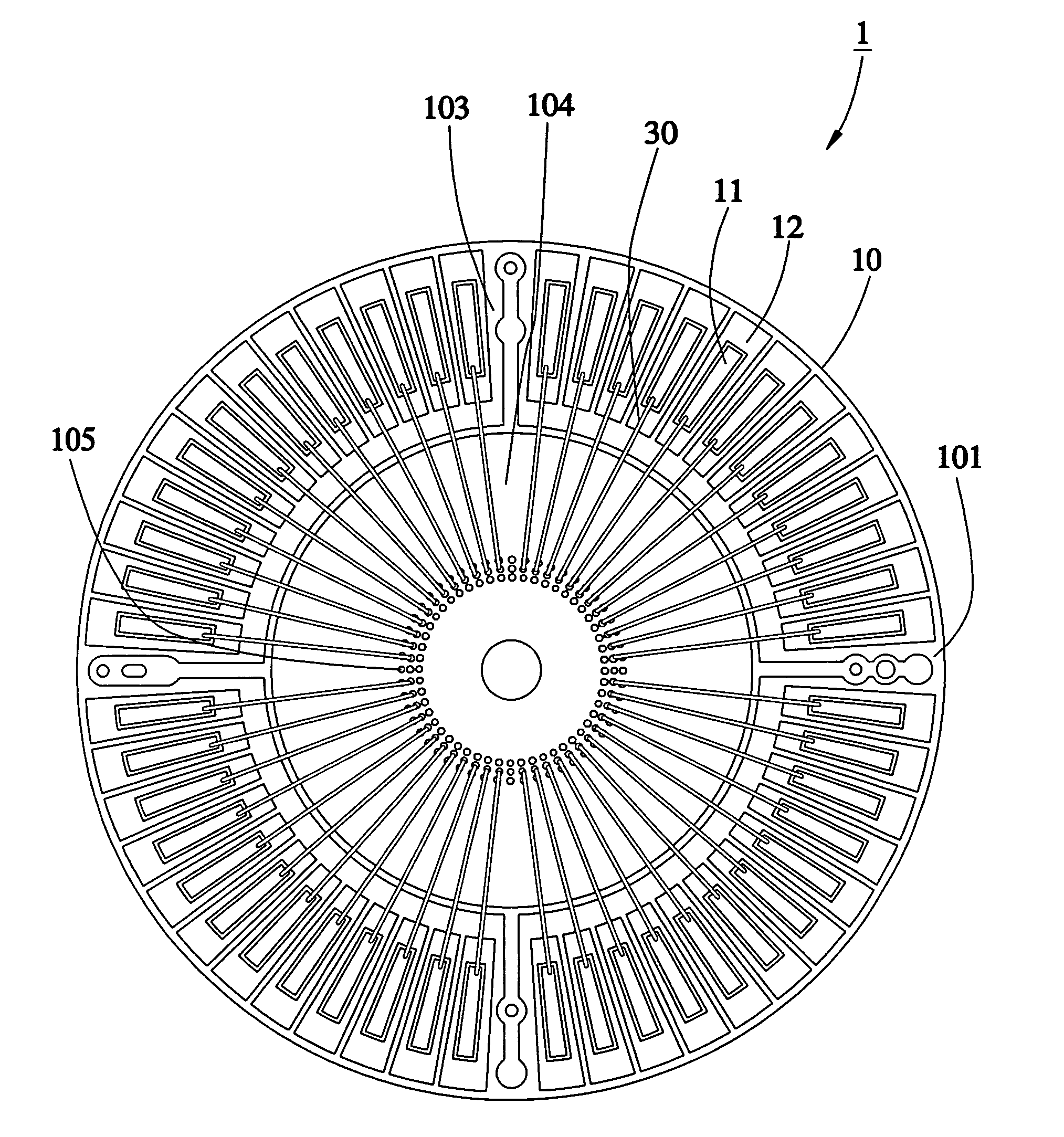
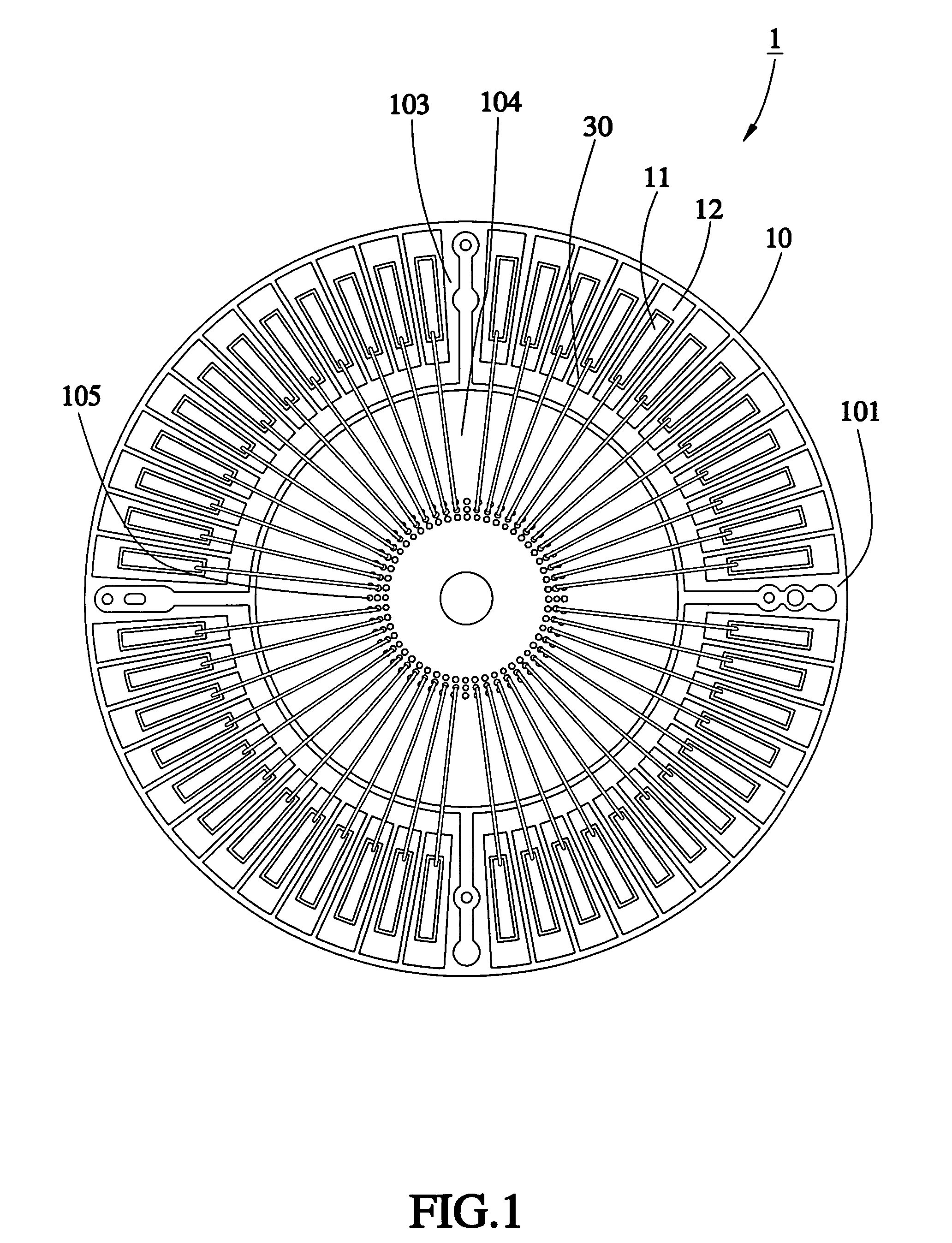
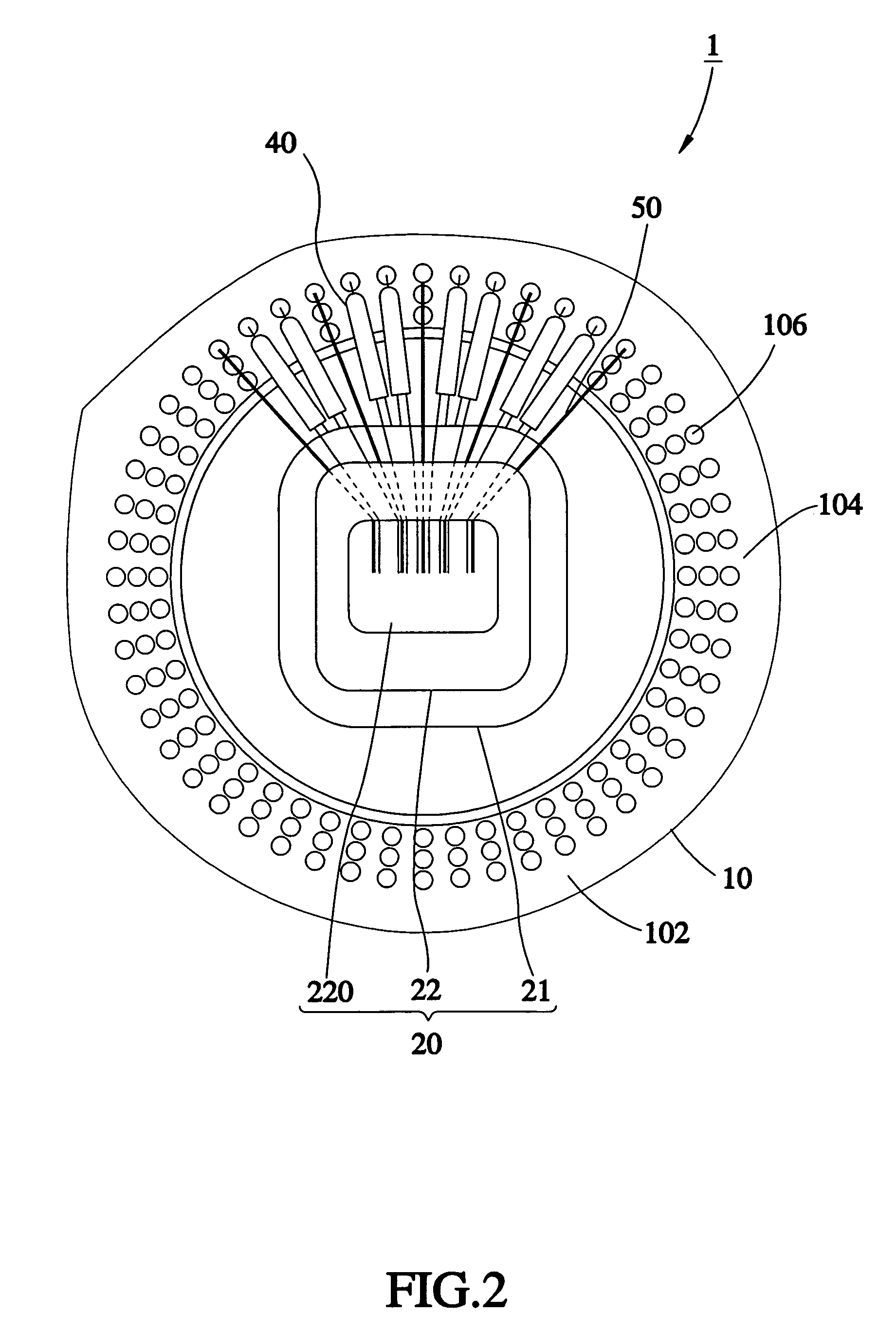
[0024]As shown in FIGS. 1-3, a high-frequency probe card 1 in accordance with a first preferred embodiment of the present invention comprises a circuit board 10, a probe holder 20, a plurality of transmission lines 30, a plurality of high-frequency probes 40, and a plurality of grounding probes 50. The circuit board 10 has a top surface 101 and a bottom surface 102, defining an annular outer test zone 103 and an annular inner jumping zone 104 concentrically disposed within the test zone 103. The circuit board 10 has arranged thereon electronic circuits. A plurality of solder pads 105 and 106 are respectively arranged on the top surface 101 and bottom surface 102 within the jumping zone 104. The electronic circuits of the circuit board 10 at the top surface 101 within the test zone 103 are electrically connected to a test machine (not shown), which is controlled to output a high-frequency test signal to the high-frequency probe card 1. The solder pads 105 at the top surface 101 are r...
PUM
 Abstract
Description
Claims
Application Information