Method of and apparatus for dispensing photoresist in manufacturing semiconductor devices or the like

a technology of photoresist and manufacturing semiconductors, applied in the direction of manufacturing tools, superimposed coating process, liquid/solution decomposition chemical coating, etc., can solve the problems of photoresist masks formed from photoresist layers, defects in the pattern formed on the wafer by the subsequent etching process, and mask defects

Inactive Publication Date: 2010-03-30
SAMSUNG ELECTRONICS CO LTD
View PDF5 Cites 4 Cited by
  • Summary
  • Abstract
  • Description
  • Claims
  • Application Information

AI Technical Summary

Benefits of technology

[0013]Another object of the present invention is to provide a method of and apparatus for delivering photoresist to a spray nozzle in a manner that prevents or minimizes the production of bubbles in the photoresist.
[0016]According to one aspect of the present invention, a bubble removal filter is disposed in the supply line downstream of the charge pump and upstream of the first filter to remove air bubbles from the photoresist. Preferably, the bubble removal filter has a housing, an inlet pipe and an outlet pipe that extend from the housing, and a membrane disposed in the housing. The inlet and outlet pipes may extend from opposite sides of the housing so as to be disposed in series. In this case, the housing has an inner diameter larger than each of the inner diameters of the inlet and outlet pipes. An exhaust pipe may be connected to the housing of the bubble removal filter so that air formed from an accumulation of the bubbles in the housing can be exhausted from the housing.

Problems solved by technology

However, even if the layer of photoresist covering the wafer W has a uniform thickness, the photomask formed from the layer of photoresist will be defective if the photoresist itself contains foreign substances.
A defective photomask will, in turn, cause defects in the pattern formed on the wafer by the subsequent etching process.
Accordingly, bubbles in the photoresist can cause defects in the mask and hence, in the pattern formed by the etching process.
In fact, even micro-bubbles entrained in the photoresist can severely influence the quality of a pattern formed according to the design rule of today's highly integrated semiconductor devices.
Thus, the rate at which the photoresist sprayed through the spraying nozzle 50 fluctuates and, as a result, the thickness of the layer of photoresist covering the wafer is not uniform.
As mentioned above, the end results are a defective mask, and defects in the pattern formed on the wafer by an etching process that uses the mask.

Method used


Image

  • Method of and apparatus for dispensing photoresist in manufacturing semiconductor devices or the like
  • Method of and apparatus for dispensing photoresist in manufacturing semiconductor devices or the like
  • Method of and apparatus for dispensing photoresist in manufacturing semiconductor devices or the like

Examples


second embodiment

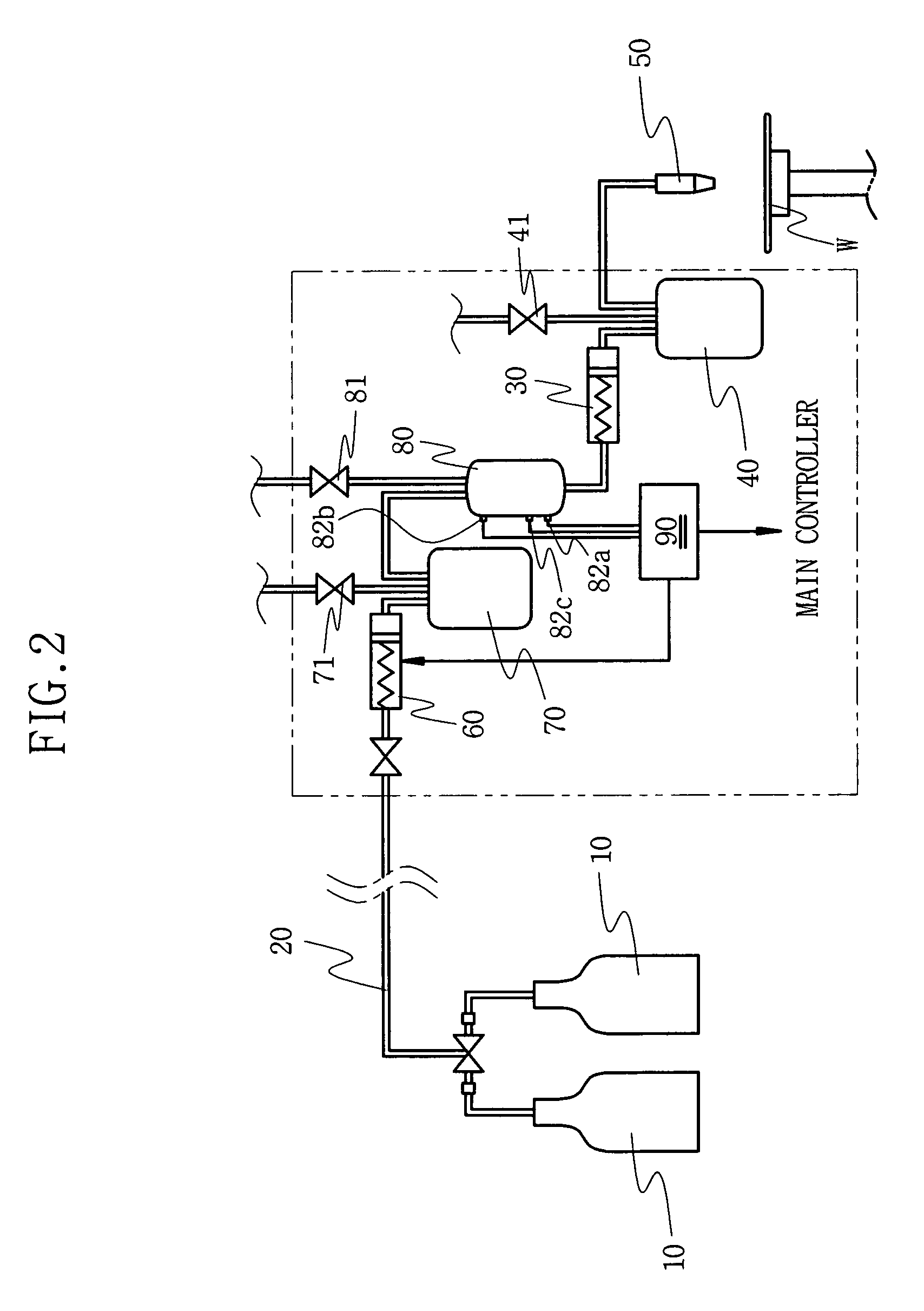
[0041]Next, a photoresist dispensing apparatus according to the present invention will be described with reference to FIG. 4.

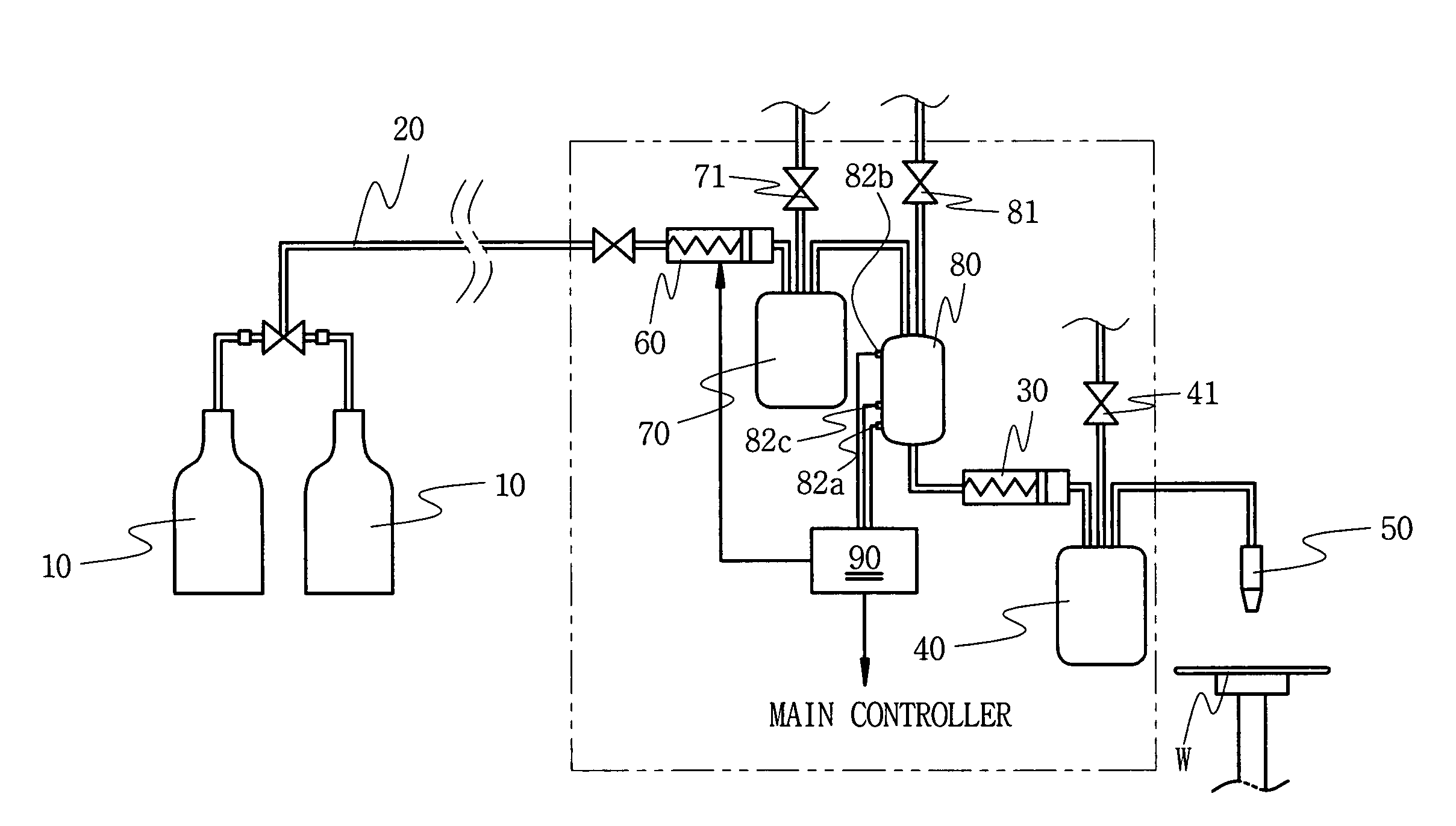
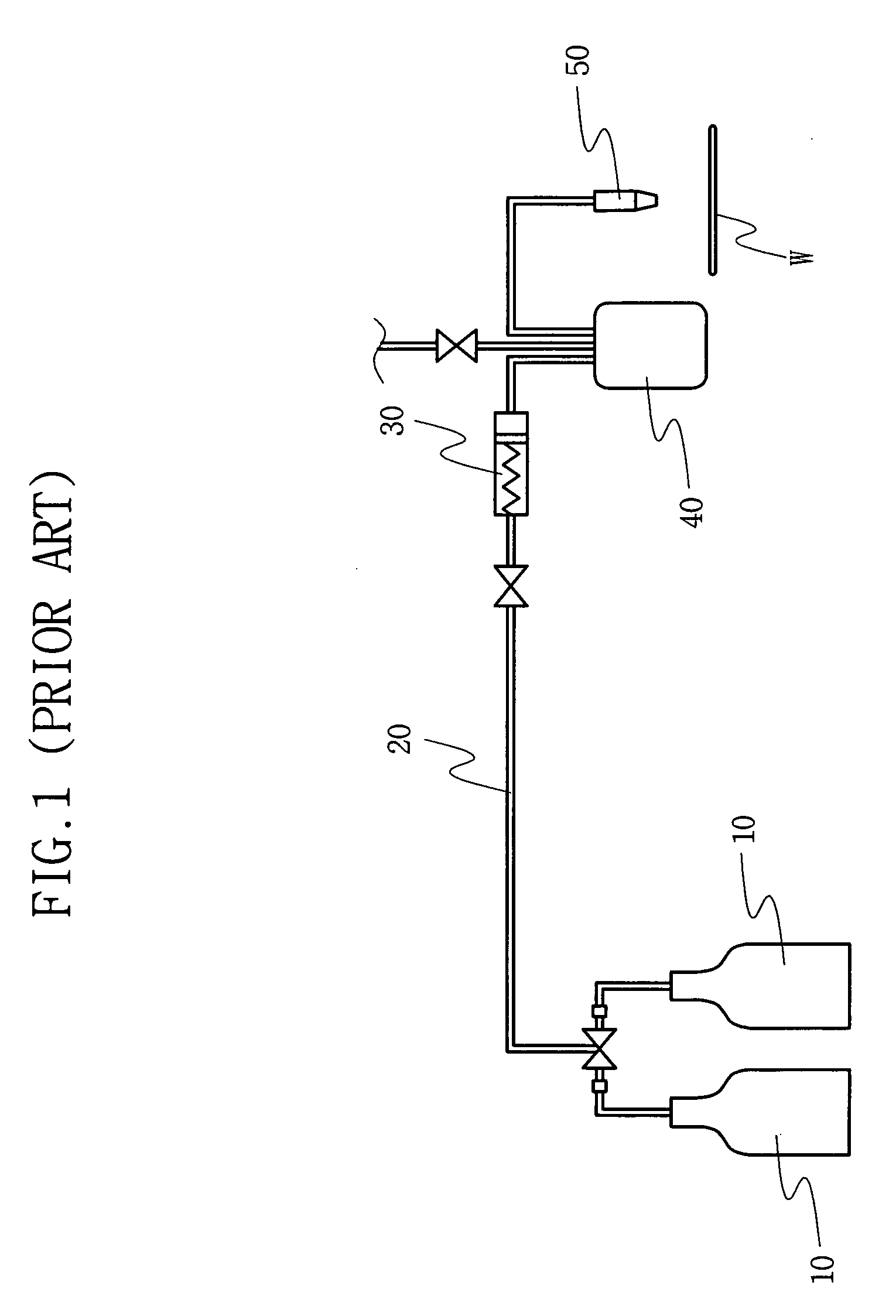
[0042]The second embodiment has a configuration similar to that of the first embodiment. Specifically, the second embodiment of the photoresist dispensing apparatus includes at least one bottle 10 for storing a given volume of photoresist, a supply line 20 connected to the at least one bottle 10, a dispensing pump 30 for drawing photoresist into the supply line 20 from the bottle 10 a foreign substance removal filter 40 downstream of the dispensing pump 30, a spray nozzle 50 by which the photoresist is sprayed uniformly onto a wafer W, and a bubble removal unit disposed within the supply line 20.

[0043]However, unlike the first embodiment, the bubble removal unit of the second embodiment includes a first charge pump 60, a first buffer tank 100, a bubble removal filter 70, a second charge pump 110 and a second buffer tank 80.

[0044]The first charge pump 60 coerce...

first embodiment

[0057]Meanwhile, the operation of the apparatus can be shut down as in the first embodiment when the apparatus is to dispense another type of photoresist and / or the bottle(s) is / are to be exchanged. In this case, photoresist in the supply line 20 and in the filters 70, 40 and the buffer tanks 100, 80 can be drained through respective drain lines by opening the valves 41, 71, 81, and 101. Again, a dedicated high capacity suction pump is used to withdraw the photoresist through the drain lines.

[0058]In such a photoresist dispensing process according to the present invention, photoresist flows more rapidly through the first charge pump 60 and the second charge pump 110 than through the dispensing pump 30, to prevent bubbles from being produced in the flow of photoresist. Regardless, any bubbles that are produced are filtered off by the bubble removal filter 70. Therefore, the foreign substance removal filter 40 is very effective at removing foreign substances from the photoresist. Thus...


PUM

PropertyMeasurementUnit
volumeaaaaaaaaaa
pressureaaaaaaaaaa
inner diameteraaaaaaaaaa

Abstract

In a photoresist dispensing apparatus for use in manufacturing a semiconductor device, to coercively emit photoresist from a bottle by using a dispensing pump and to pass it through a supply line and a filter to obtain a filtering operation, and to spray the filtered photoresist to a wafer through a spraying nozzle; a bubble removal unit is equipped with the supply line, before the dispensing pump. Large and micro bubbles generated in the midst of flow of photoresist, and foreign substances, are substantially filtered off so as to supply photoresist of a good quality. A floating load in a foreign substance removal filter is substantially removed, thus spraying photoresist under an always uniform and stabilized pressure by using a dispensing pump, to cover a wafer with photoresist in a uniform thickness and obtain a precise pattern formation.

Description

BACKGROUND OF THE INVENTION[0001]1. Field of the Invention[0002]The present invention relates to the manufacturing of semiconductor devices or the like. More particularly, the present invention relates to the dispensing of photoresist onto a wafer or other substrate.[0003]2. Description of the Related Art[0004]In general, the manufacturing of semiconductor devices involves subjecting a wafer to a series of processes such as diffusion, photolithography, etching, ion implantation and deposition processes. In particular, the photolithography and etching processes are carried out to form a pattern, e.g., a circuit pattern, on the wafer. The photolithography process entails forming a mask on a wafer to expose portions of a layer underlying the mask. The etching process entails removing the portions of the layer exposed by the mask.[0005]The photolithography process begins by dispensing a chemical, namely a photoresist, onto a surface on a wafer, and forming a uniform thin layer of the ph...

Claims


Application Information

Patent Timeline
Patent Type & Authority Patents(United States)
IPC IPC(8): B05C5/02
CPCG03F7/016B01D19/0031B05C11/1002G03F7/16
Inventor LEE, JONG-HAWPARK, JIN-JUN
Owner SAMSUNG ELECTRONICS CO LTD
Why Eureka
Try Eureka