

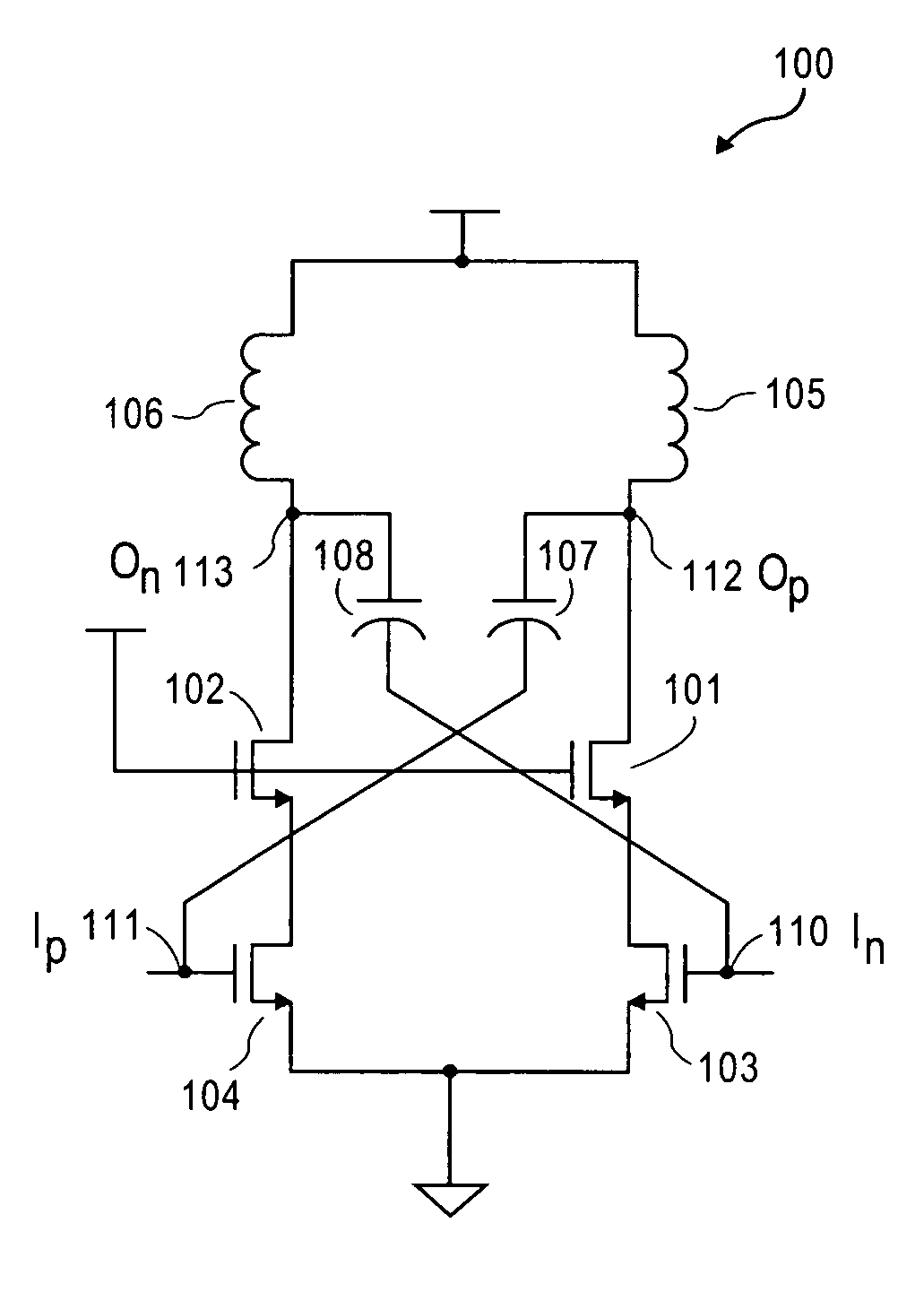
Gain boosting RF gain stage with cross-coupled capacitors
a capacitor and gain boost technology, applied in the field of communication devices, can solve the problems of reducing the overall signal-to-noise ratio of the amplifier, reducing the resistance associated with the inductor, and reducing the overall q and/or the gain of the stag
- Summary
- Abstract
- Description
- Claims
- Application Information
AI Technical Summary
Benefits of technology
Problems solved by technology
Method used
Image

Examples
Embodiment Construction
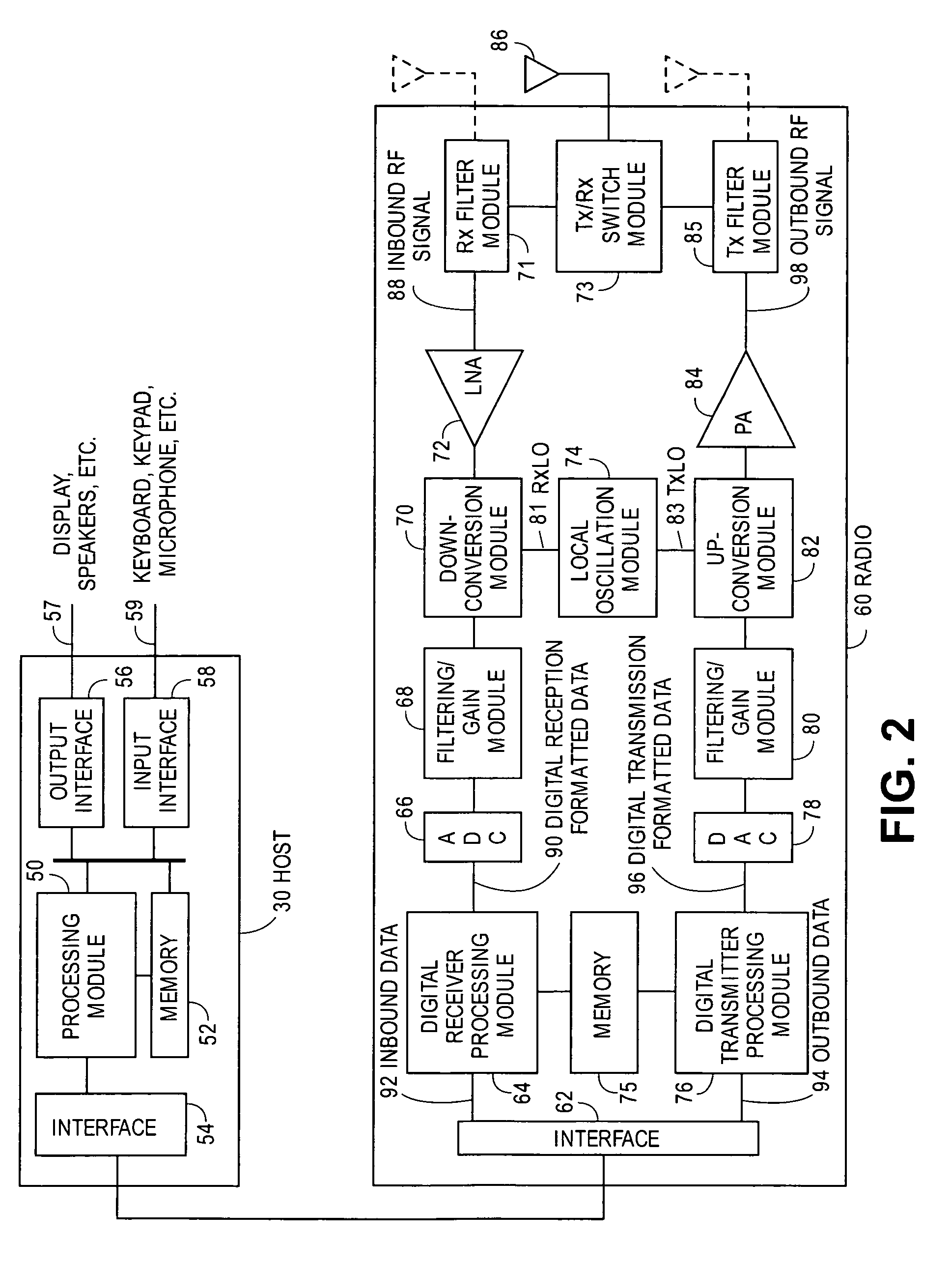
[0019]The embodiments of the present invention may be practiced in a variety of settings that implement a radio frequency (RF) amplifier stage.
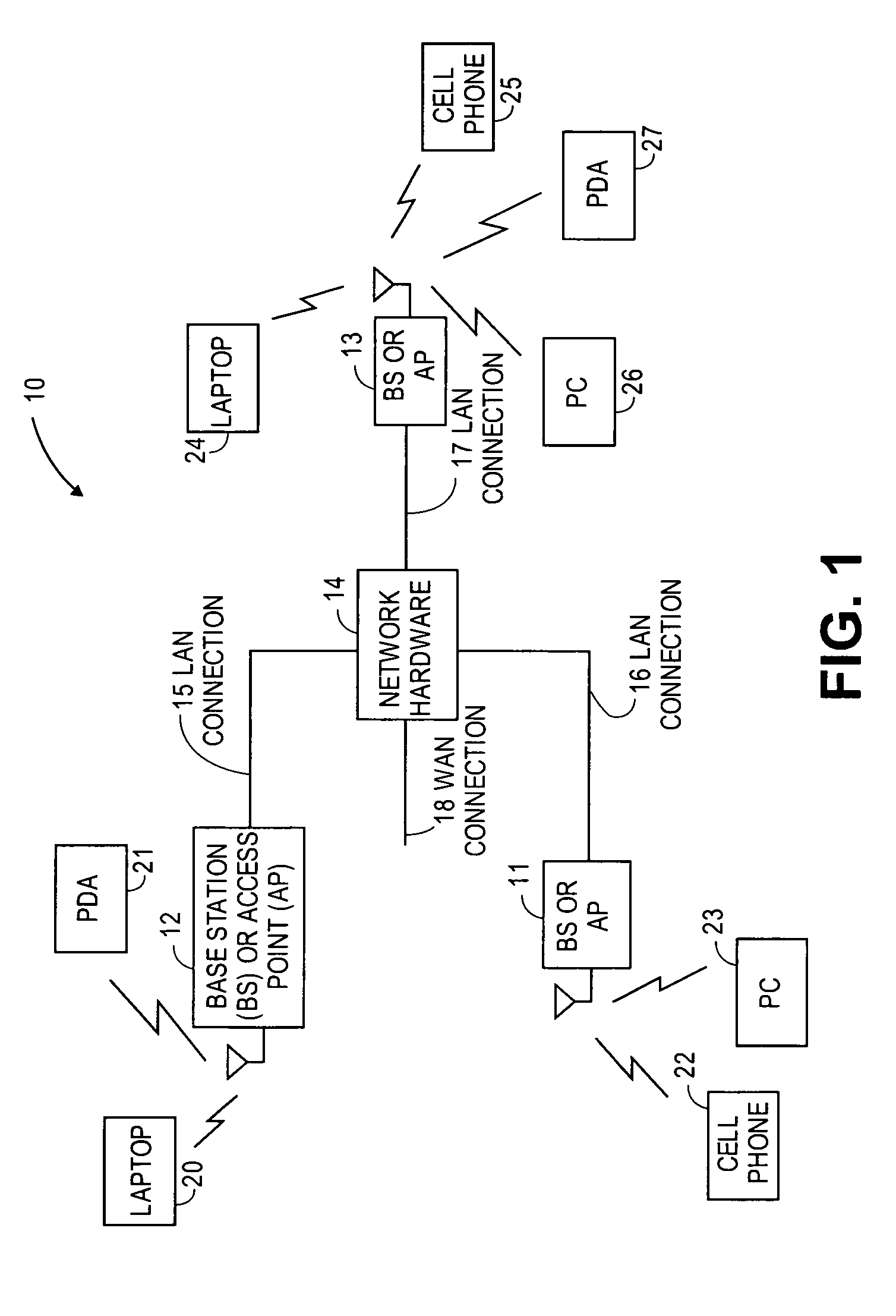
[0020]FIG. 1 is a schematic block diagram illustrating a communication system 10 that includes a plurality of base stations (BS) and / or access points (AP) 11-13, a plurality of wireless communication devices 20-27 and a network hardware component 14. Wireless communication devices 20-27 may be laptop host computers 20 and 24, personal digital assistant hosts 21 and 27, personal computer hosts 23 and 26, cellular telephone hosts 22 and 25, and / or any other type of device that supports wireless communications. The details of the wireless communication devices will be described with reference to FIG. 2.
[0021]Base stations or access points 11-13 may be operably coupled to network hardware 14 via respective local area network (LAN) connections 15-17. Network hardware 14, which may be a router, switch, bridge, modem, system controller, et cetera, m...
PUM
 Abstract
Description
Claims
Application Information