Thin film transistor having silicon nanowire and method of fabricating the same

a thin film transistor and silicon nanowire technology, applied in the field of flat panel display, can solve the problems of increasing process time and production cost, amorphous silicon is unsuitable for a large size lcd, and manufacturing array substrates, and achieves the effect of simple process and stable operation

Inactive Publication Date: 2010-04-27
LG DISPLAY CO LTD
View PDF9 Cites 62 Cited by
  • Summary
  • Abstract
  • Description
  • Claims
  • Application Information

AI Technical Summary

Benefits of technology

[0043]An advantage of the present invention is to provide a TFT including a silicon nanowire that can have a stable operation.
[0044]Another advantage of the present invention is to provide a TFT including a silicon nanowire that does not interfere with efficient processing.
[0045]Another advantage of the present invention is to provide a method of fabricating a TFT including a silicon nanowire that can form a TFT including a silicon nanowire by a simpler process than the related art.

Problems solved by technology

Although the semiconductor layer 57 of the inverted staggered TFT T includes amorphous silicon, in fact, the amorphous silicon is unsuitable for a large size LCD.
Therefore, manufacturing the array substrate increase the process time and the production cost.
These events result in device operation instability.

Method used


Image

  • Thin film transistor having silicon nanowire and method of fabricating the same
  • Thin film transistor having silicon nanowire and method of fabricating the same
  • Thin film transistor having silicon nanowire and method of fabricating the same

Examples


first embodiment

[0066]A first embodiment according to the present invention includes a silicon nanowire as an active layer, and source and drain electrodes formed of the same material as the gate electrode through a same process.

[0067]FIGS. 6A to 6E are schematic cross-sectional views showing an array substrate having a TFT including a silicon nanowire in accordance with a manufacturing process according to a first embodiment of the present invention.

[0068]In FIG. 6A, a silicon nanowire 102 is disposed on a substrate 100. Although not shown, for example, the silicon nanowire 102 is formed by depositing a catalyzer on a semiconductor substrate (not shown) and crystallizing the catalyzer using a reactive gas including silicon. This silicon nanowire 102 may be sprayed on the substrate 100 after depositing and crystallizing on the semiconductor substrate. Further, the silicon nanowire 102 has a rod shape as shown in FIG. 6A. Although not shown, the silicon nanowire 102 includes a core of a semiconducto...
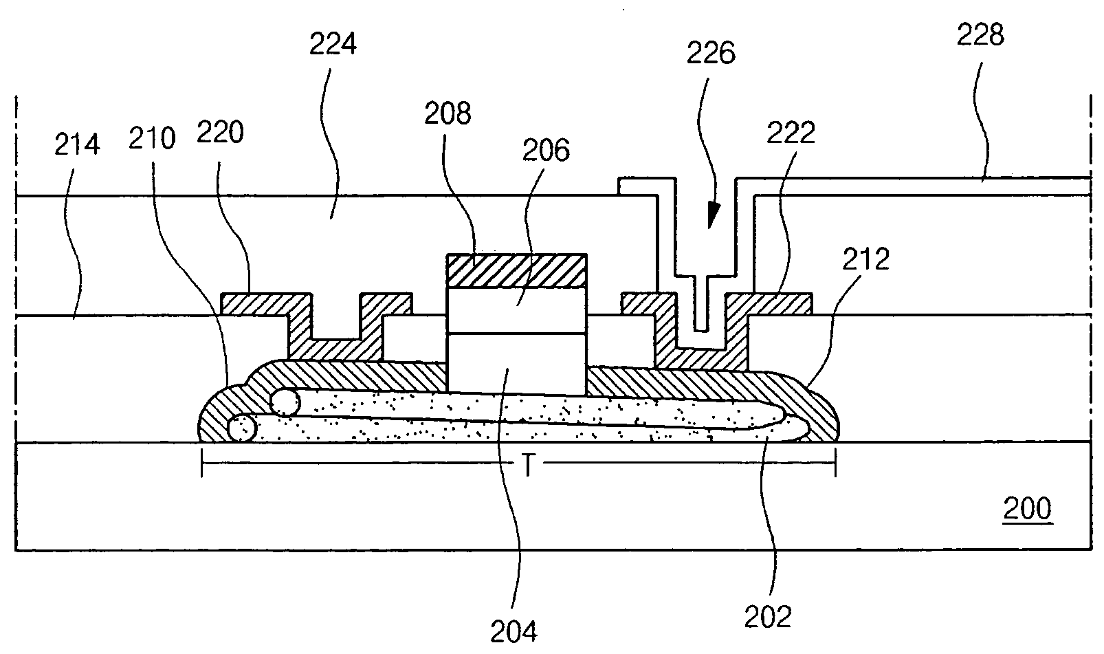
second embodiment

[0083]A second embodiment has a feature such that a silicon nanowire is formed by spraying on a substrate.

[0084]FIGS. 7A to 7F are schematic cross sectional views showing an array substrate including a TFT having a silicon nanowire in accordance with a manufacturing process according to a second embodiment of the present invention.

[0085]In FIG. 7A, a silicon nanowire 202 is disposed on a substrate 200, for example, a solvent 201 having the silicon nanowire 202 and surfactant (not shown) is prepared and the solvent 201 may be coated by spraying on the substrate 200. For example, the silicon nanowire 202 may be formed by depositing a catalyzer having a nanoscale size on a semiconductor substrate (not shown) and by crystallizing the catalyzer using a reactive gas including silicon before preparing the solvent 201.

[0086]Substantially, although not shown, the silicon nanowire 202 includes a core and an insulating layer surrounding the core so as to form a coaxial structure therebetween. ...


PUM

PropertyMeasurementUnit
sizeaaaaaaaaaa
insulatingaaaaaaaaaa
temperatureaaaaaaaaaa

Abstract

A thin film transistor includes: a silicon nanowire on a substrate, the silicon nanowire having a central portion and both side portions of the central portion; a gate electrode on the central portion; and a source electrode and a drain electrode spaced apart from the source electrode on the both side portions, the source electrode and the drain electrode electrically connected to the silicon nanowire, respectively.

Description

[0001]This application claims the benefit of Korean Patent Application No. 10-2005-0029120, filed on Apr. 7, 2005, which is hereby incorporated by reference for all purposes as if fully set forth herein.BACKGROUND OF THE INVENTION[0002]1. Field of the Invention[0003]The present invention relates to a flat panel display (FPD), and more particularly to a thin film transistor (TFT) for a FPD and a manufacturing method thereof.[0004]2. Discussion of the Related Art[0005]Generally, the FPD includes a liquid crystal display (LCD) device, a plasma display panel (PDP) and an organic electroluminescent display device (OLED) or the like. Here, the TFT is utilized as a switching element or a driving element of the FPD.[0006]FIG. 1 is a schematic view of a structure of an LCD according to the related art.[0007]In FIG. 1, an LCD 3 includes upper and lower substrates 5 and 22 facing each other and a liquid crystal layer 11 between the upper and lower substrates 5 and 22.[0008]A gate line 12 and a...

Claims


Application Information

Patent Timeline
Patent Type & Authority Patents(United States)
IPC IPC(8): H01L21/00
CPCB82Y10/00H01L27/1214H01L29/0665H01L29/0673H01L29/4908H01L29/66757H01L29/78696H01L29/775H01L29/41733Y10S977/762H01L27/1222H01L27/127A62C2/16A62C2/246
Inventor CHAE, GEE-SUNGPARK, MI-KYUNG
Owner LG DISPLAY CO LTD
Why Eureka
Try Eureka